
555 sound logic level probe
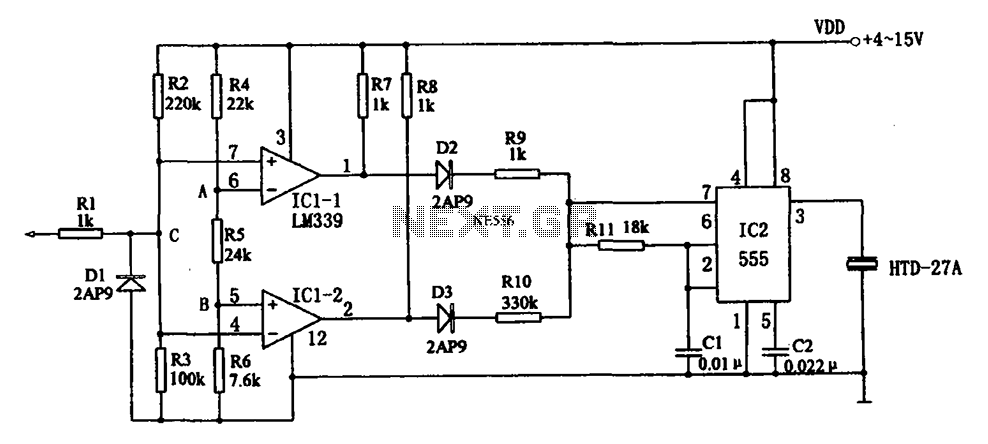
The acoustic logic level probe circuit is designed to provide an efficient means of assessing digital logic levels in TTL and CMOS devices through auditory feedback. The integration of a voltage comparator (LM339) allows for precise voltage level detection, while the multivibrator configuration facilitates the generation of distinct frequencies corresponding to the logic levels. The use of piezoelectric ceramics (HTD) as the sound-emitting element enhances the circuit's ability to provide audible indications of detected levels.
The voltage divider network composed of resistors R2 and R3 is crucial for establishing reference voltages necessary for the comparator's operation. By setting the voltage at point C to 1.9V, the circuit can differentiate between high and low logic levels effectively. The operation of diodes D2 and D3 plays a significant role in controlling the activation of the oscillator IC2, ensuring that sound generation occurs only when appropriate logic levels are detected.
The charging and discharging of capacitor C1 through resistors R9, R10, and R11 is fundamental in determining the oscillation frequencies. The calculated frequencies (approximately 4 kHz for high levels and 700 Hz for low levels) provide a clear auditory distinction between the logic states, allowing for immediate identification of the signal type. The ability to mix tones or produce tremolo effects when bursts are detected enhances the user experience, making the probe not only functional but also engaging.
Overall, this circuit exemplifies an innovative approach to logic level detection, utilizing auditory signals to convey information about digital states, making it a valuable tool for electronics engineers and technicians working with digital circuits. As shown for the acoustic logic level probe circuit. The probe consists of a voltage comparator, multivibrator, piezoelectric ceramics HTD and other components. Wherein the com position of the latter two audio circuit to the frequency of the sound level to determine the level of TTL or CMOS device level. Voltage comparator LM339 (IC1) in IC1-1, IC1-2 each 1/4 LM339. Divider network R2, R3 so that when VDD 6V voltage dividing point C is Vc F1.9V, which is lower than the reference voltage IC1-1, but higher than the reference voltage IC1-1, it usually diode D2, D3 are closing, oscillator IC2 does not work.
When the probe contacts the high, low, or pulse, is used to detect high IC1, IC2 for detecting low-level output signal corresponding driven D2, D3 conduction, and through R9, R10, R11 C1 to be charging the IC2 start-up, promote HTD sound. When the probe contacts the high level, IC1-1 output signal so that D2 is turned on, and through R9, R11 on the C1 is charged.
Oscillator start-up, the corresponding oscillation frequency fH 1.44/(R10 + 2R11) C1, the icon parameter corresponding frequency of approximately 4kHz. When the probe contacts the low level, the corresponding D3 conduction, C1 through R10, R11 for charging the corresponding oscillation frequency of the oscillation circuit after start-up is fL 1.44/(R10 + 2R11) C1, the frequency corresponding to the icon parameter is about to 700Hz.
When a burst is detected, the corresponding HTD emit sound mixing two or given tremolo sound. The high-frequency sound judgment circuit is high; low frequency sound judgment low; fat vibrato said probe is a series of pulses, thus realizing the logic level detection.
Related Circuits
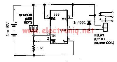
The water sensor circuit utilizes a 555 timer configuration along with standard electronic components. It consists of two metal electrodes positioned closely enough that a drop of water can create a conductive bridge between them. In cases where the...
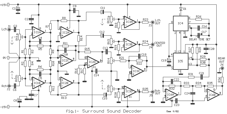
The particular circuit does not have the requirement to replace the trade decoders Surround, because they have many more facilities and possibilities. It gives, however, the possibility in many trials with this article of decoding. The coding in Stereo...
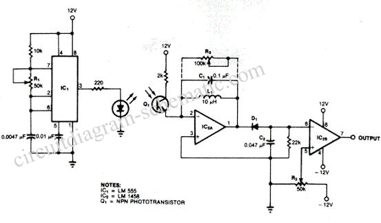
The following circuit illustrates an LM555 integrated circuit (IC) motion detector utilizing infrared sensors. Features include the generation of an infrared pulse modulation at 5 kHz, along with bandwidth control. The LM555 timer IC is a versatile component widely used...
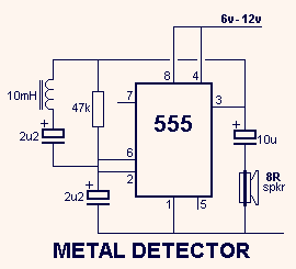
This circuit detects metal and also magnets. When a magnet is brought close to the 10mH choke, the output frequency changes. The circuit operates on the principle of inductance variation in response to the presence of a magnetic field. The...
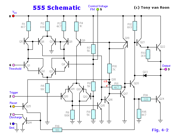
The 555 timer IC was first introduced around 1971 by the Signetics Corporation as the SE555/NE555 and was referred to as "The IC Time Machine." It was the first commercially available timer IC, providing circuit designers and hobbyists with...
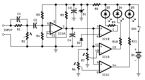
This circuit indicates audio output power using three LEDs. It serves as a useful addition to an amplifier. The audio output power indicator circuit is designed to visually represent the power level of an audio amplifier through the use of...
Warning: include(partials/cookie-banner.php): Failed to open stream: Permission denied in /var/www/html/nextgr/view-circuit.php on line 713
Warning: include(): Failed opening 'partials/cookie-banner.php' for inclusion (include_path='.:/usr/share/php') in /var/www/html/nextgr/view-circuit.php on line 713