
0-50V 1A Laboratory Power Supply

The laboratory power supply described utilizes the LM10 op-amp to achieve precise voltage regulation and adjustable output. The LM10 is a versatile device that allows for a wide range of output voltages to be set through external resistors connected to its feedback loop. By configuring the gain of the op-amp, the desired output voltage can be adjusted continuously, providing flexibility for various applications.
In addition to voltage regulation, the circuit incorporates a current limiting feature to enhance safety. This is crucial in preventing damage to both the power supply and the connected load. The current limiter can be implemented using a simple resistor in series with the load, and a transistor that monitors the current flow. When the current exceeds a predetermined threshold, the transistor activates, reducing the output voltage to maintain safe operating conditions.
The schematic diagram typically includes the LM10 op-amp, a voltage reference source, and the necessary passive components such as resistors and capacitors for stability and filtering. The power supply design may also feature additional elements such as LED indicators for power status and output voltage levels, as well as protection diodes to safeguard against reverse polarity connections.
Overall, this laboratory power supply design is robust, adaptable, and suitable for a variety of electronic experiments and testing environments, ensuring reliable performance across a wide range of applications.Laboratory power supply is characterized by its wide adjustable voltage range and its robustness. Continuous voltage adjustment is necessary, as well as current limiter for safety and robustness. You can build suitable one using LM10 op-amp and voltage source IC as shown in the schematic diagram below: 🔗 External reference
Related Circuits
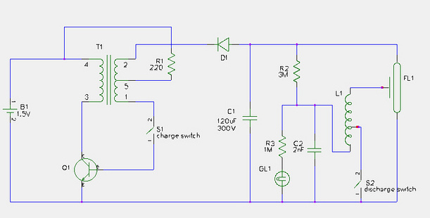
This document provides a step-by-step guide for modifying a disposable camera flash unit to serve as a power supply for a Geiger tube. The process involves removing the flash tube and trigger transformer from the circuit board by gently...
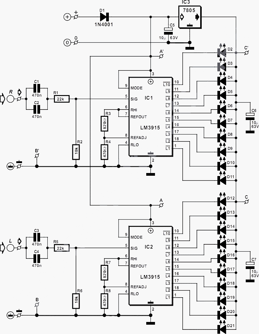
This circuit detects the AC audio voltage supplied to car radio loudspeakers and visually represents it as power using an LED bar graph, creating an appealing visual effect. It is designed to accommodate typical car radio output power ranges...

This chapter presents detailed schematics for various power supplies compatible with commonly available Ar/Kr ion tubes in the surplus market. It includes examples of commercial designs such as the Omnichrome 150R and 532 head, Lexel 88 and head, alongside...
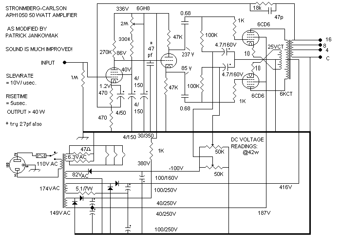
If 40 watts RMS from 20Hz to 30KHz +/-1.5 dB is appealing, this experiment may be of interest. A significant issue with public address equipment is the use of audio output transformers that lack sufficient iron to manage lower...
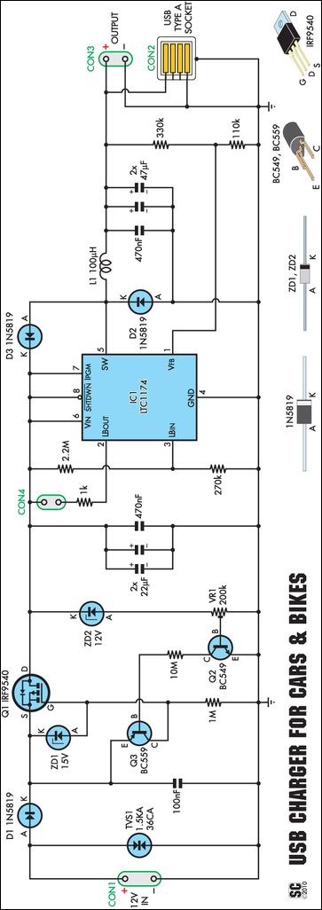
An efficient USB charger designed to operate from a 12V car battery, achieving up to 89% efficiency and capable of charging USB devices at currents up to 525mA. It does not drain the battery if left permanently connected, provided...

The following circuit illustrates a 2000W Power Amplifier Circuit Diagram. This circuit utilizes the BC560C transistor. Features include a robust design. The 2000W power amplifier circuit is designed to deliver high output power suitable for various applications, including audio amplification...