
1.3W Linear Power Amplifier
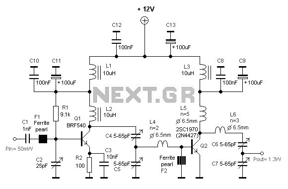
Transistor Q1 will act as a buffer amplifier because it is not intended to load the previous stage too much. The input RF signal passes through C1 and F1, which is a small ferrite pearl where the wire just passes through. F1 with C2 will act as an impedance matching for Q1. F1 can be substituted with a coil as L4, but tests have shown that the ferrite pearls provide the best performance. L2 is not a critical component, and any coil from 2-10uH will suffice. Q1 will amplify the input signal from 50mW to about 200mW. While Q1 can amplify more, 200mW is sufficient for the final transistor. If higher power is desired, the resistor R2 can be decreased.
In Q2, a ferrite pearl F2 is located at the base to emitter. This ferrite pearl is used to set the DC voltage to zero and provide high impedance for RF signals. The wire is wound four times around this small ferrite pearl and can be substituted with a coil of 1uH or more. This amplifier is based on the transistors 2SC1970 and 2N4427, with an output power of approximately 1.3W and an input driving power of 30-50mW. Other transistors like 2SC1971 can be utilized for greater output power. The 1.3W output is sufficient to transmit RF signals effectively, and a good 50 ohm resistor should be used as a dummy load, rated to handle 5-10W to avoid overheating.
Capacitors C4, C5, and inductor L4 form an input matching network for the transistor. At the output of the final transistor Q2, two coils L5 and L6 are present. Together with capacitors C6 and C7, they form an impedance matching network for both the antenna and the transistor. This configuration is critical for ensuring efficient signal transmission and preventing damage to the components involved. Proper attention to component specifications and ratings is essential for reliable operation of the amplifier circuit.Some amplifier is based around a RF transistor. In my case I will use a common NPN RF transistor called 2SC1970. You can also use other transistors like 2N4427 and some others. Check datasheets to se how much power the transistor can handle. 2SC1970 will handle 1.3W and 2SC1971 up to 6W. Most transistor has a power gain of 10dB meaning 10 times power amplification. This is the reason why you must use several stages to achieve a strong transmitter. In this construction we are getting higher power then ever and you must be careful with the transistor. A 50 ohm dummy load MUST be used while testing, else the final transistor will break. An antenna can be used but the antenna must be properly made else the transistor will break. More about that later. In all RF system and specially in RF amplifiers, it is very important to have a stable power supply and making sure you won't get any RF out on the power line. The Capacitor C12 and C13 will stabilise the DC power supply. L1, C10, C11 and L3 with C8, C9 will also prevent RF from leaking out to the powerline and cause oscillation or disturbances.
L1 and L3 should be ferrite chokes or inductance's about 1 to 10 uH. Transistor Q1 will act as a buffer amplifier, because I don't want to load the previous stage to much. The input RF signal is passin C1 and F1 which is a small ferrite pearl where the wire just passing through.
F1 with C2 will act as an impedance matching for Q1. F1 can be substituted with a coil as L4, but in my test I found that the ferrite pearls gave best performances. L2 is nit a critical component and any coil from 2-10uH will do the job. Q1 will amplify the input signal from 50mW to about 200mW. Q1 can amplify much more, but It doesn't need to do that because 200mW is good for the final transistor.
If you want higher power you can decrease the resistor R2. If you look at Q2 you will also find a ferrite pearl F2 at the base to emitter. This ferrite pearls is to set the DC voltage to zero and be a high impedance for RF signals. I wounded the wire 4 times around this small ferrite pearl. You can substitute it with a coil of 1uH or more. This amplifier is based on the transistor 2SC1970 and 2N4427. The output power is about 1.3W and the input driving power is 30-50mW. You can use other transistor as 2SC1971 and get much more output power. 1.3W will still get your RF signal quit far and I advice you to use a good 50 ohm resistor as dummy load. Make sure it can take up to 5-10W, else it will be a hot resistor. C4, C5 and L4 forms an input matching unit for the transistor. Not much we can do about that At the output of the final transistor Q2 you will find 2 coils L5 and L6.
Together with C6 and C7, they form an impedance unit for the antenna and also for the transistor. 🔗 External reference
Related Circuits

This preamplifier amplifies the signal from a microphone, an amplifier so that it can be further strengthened. The circuit supplies an output signal line. With two transistors, it is not difficult to build such a circuit. The amplifier produces...
Simple circuit, no ICs required, 12V battery operation. This circuit was requested by several correspondents. Its purpose was to obtain more power than the standard configurations allow. This circuit design utilizes a 12V battery as the primary power source and...

This is an adjustable and regulated power supply with an output voltage range of 3V to 30V and a current supply capability of up to 3A. This circuit is equipped with short circuit protection and overload protection. The adjustable power...
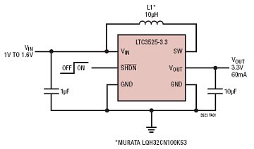
The LTC3525-3/LTC3525-3.3/LTC3525-5 are high-efficiency synchronous step-up DC/DC converters with output disconnect capability that can operate with an input voltage as low as 1V. These converters provide a compact and efficient alternative to charge pumps for single-cell or dual-cell alkaline...

This Class A preamplifier features a symmetrical design. The input differential stages utilize dual transistors, T1 and T2. Polarization correction is crucial due to amplification discrepancies and is managed by transistor T12. Potentiometer P2 adjusts the output voltage to...
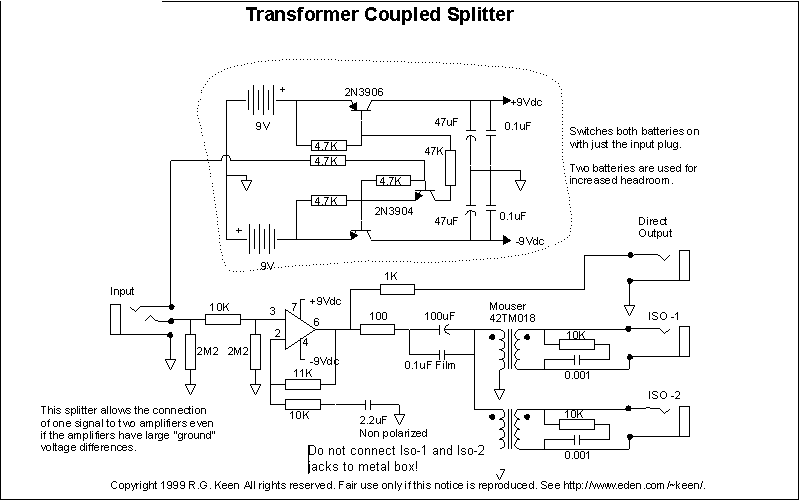
An active amplified transformer isolated signal splitter that enables a hum-free connection of one guitar to multiple amplifiers, while also providing a direct output. This includes a discussion on using audio transformers for equipment interconnections and mentions line-level transformers...