
10 Way Electronic Switch
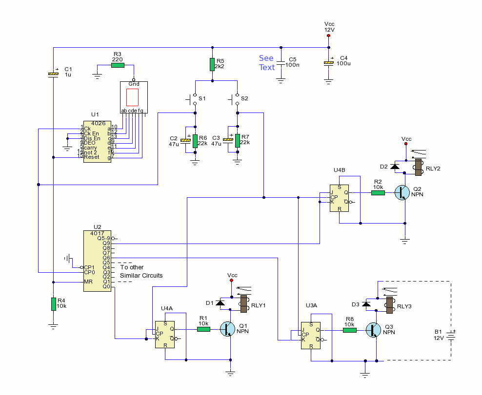
The circuit design integrates a CMOS4017 decade counter and a CMOS4027 JK flip-flop to create a versatile output control system. The operation begins with the charging of capacitor C1, which ensures that both U1 and U2 are reset, setting the initial state of the system. The 4017 IC is programmed to count from 0 to 9, with each output corresponding to a specific state displayed on the seven-segment display driven by U1. The use of switch S1 allows for manual incrementing of the count, facilitating user interaction with the system.
The JK flip-flop configuration provided by the CMOS4027 adds flexibility to the output control, enabling each output to be independently set or reset. This is particularly useful in applications where multiple outputs need to be managed without interference. The inclusion of switch S2 allows for real-time toggling of the outputs, enhancing the system's responsiveness to user commands.
Transistor drivers are employed to manage larger loads through relays, providing isolation and protection for the control circuit from high-power applications. The choice of general-purpose NPN transistors ensures that the circuit can be easily assembled with commonly available components. The schematic's design also emphasizes ease of understanding, with clear labeling and logical flow, making it accessible for both novice and experienced electronics engineers.
In summary, this circuit exemplifies a practical application of digital counting and control using CMOS technology, showcasing the integration of decade counters and flip-flops to achieve a reliable and user-friendly output management system. The design considerations for power management and component selection further enhance the circuit's functionality and adaptability to various applications.The schematic is shown above, and two switches S1 and S2 are used to control the outputs. The main work is done by U2 a CMOS4017 decade counter divider IC. At switch on, C1 is quickly charged by R4 and a brief reset pulse is applied to to the reset pins of both U1 and U2. This results in U1, a 7 segment display display driver and decade counter sh owing "zero" on the 7 segment display and pin 3 (which is the output zero) of the 4017 becoming high. Each time S1 is pressed the clock input of U2 is incremented, by one count and the display and 4017 will cycle through all 10 outputs.
A separate reset switch is not provided as the display reads the currently selected output. Each output can be toggled (set or reset) independently by the use of a JK flip flop, a CMOS4027. When the 4017 is on a particular output, for example zero, then the controlled circuit can be turned on or off using switch S2. To latch the output a type JK flip-flop is used at each of the ten outputs. The 4027 contains two JK flip flops, and only one flip flop is required per output. If you only required 5 outputs, then only three 4027 IC`s are required. Three 4027 would give you six JK flip flops, the unused flip flop should have all unused inputs tied to ground.
The circuit works as follows. When the 4017 is at output zero, pin 3 will be high. This enables both JK inputs of the flip flop (U4A at output zero) and the circuit can then be toggled via pulses applied from switch S2. The `Q` output of each flip-flop drives and NPN transistor and then a small relay. The NPN transistors can be any general purpose type, e. g. 2N2222, BC108, BC548 etc. The relay allows external loads of different voltage and current to this circuit to be controlled. Please note that VDD and VSS represent the drain and source power connections. The CMOS 4027 contains two JK Flip Flops, the pins S1, R1, J1, K1, CP1 represent the set, reset, J and K inputs and clock pulse inputs for one half of the 4027.
The other flip flop is represented as S2, R2, etc. In the diagram U3A represents one JK flip flop or half of a 4027, and U4A and U4B use both JK flip flops or one complete 4027. For clarity, the schematic is drawn with outputs, zero, six and nine shown only. The pinouts for the CMOS IC`s 4017 and 4026 can be also be found in the practical section. If required, the external circuits power supply can be used to power the driver transistor and relay.
This is shown on output 6, the dotted lines representing the power coming from an external battery. The only other requirement here is that the external circuits common negative terminal is tied to this circuits common chassis (negative) terminal. 🔗 External reference
Related Circuits
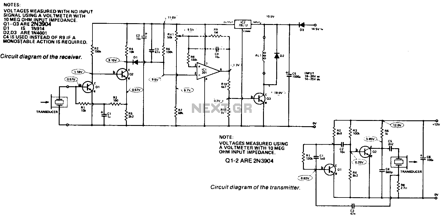
Receiver. The output from the transducer is amplified by Q1 and Q2, and rectified by D1. The voltage on pin 2 of IC1 will become more negative as the input signal increases. IC1 is utilized as a comparator, comparing...
The switcher output connects to the single vertical input of the oscilloscope, while a sync line from one of the inputs is routed to the oscilloscope's external-sync input. The frequency response of the input amplifiers reaches 300 kHz across...
This circuit employs a CA3240 dual BiMOS operational amplifier to detect small currents that flow between the contact points on a touch plate. The high input impedance of the CA3240 enables the use of 1-megaohm resistors in series with...
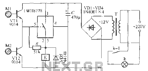
The Rw A77S power system utilizes an integrated circuit fabrication design featuring a dual touch light switch. It employs a transformer (T) for power conversion, a rectifier (VD4), and a capacitor (C) for filtering, resulting in a 12V DC...
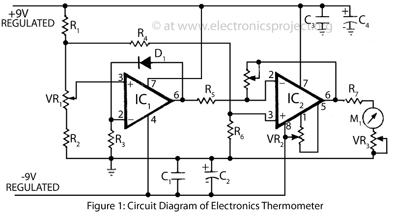
A clinical thermometer is typically used by doctors due to its complex reading mechanism. This circuit represents an electronic thermometer designed to measure a wide temperature range from -200°C to 1250°C. This single circuit electronic thermometer is capable of...
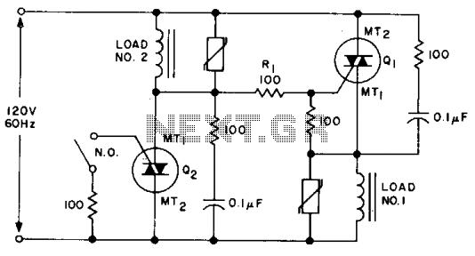
An SPDT solid-state relay is illustrated. When voltage is applied, Q1 will activate, powering load #1, as the full line voltage is present across Q2, providing gate current through R1. When switch S1 is closed, Q2 activates, removing the...