
1024kHz and 4kHz square-wave output circuit

The SJT circuit operates at a frequency of 1024 kHz, utilizing a crystal oscillator to generate a stable and precise frequency output. The crystal oscillator is a key component in this design, as it provides the necessary frequency stability through its inherent resonant properties. The output from the oscillator is typically low in amplitude, which necessitates the inclusion of a buffering stage to ensure that the signal can be effectively utilized in subsequent stages of the circuit.
The transistor VT1 serves as a buffer amplifier, which isolates the oscillator from the load while providing amplification to the output signal. The base bias resistor R2 is crucial for establishing the correct biasing conditions for the transistor, ensuring that it operates in the active region. This resistor is selected based on the desired base current, which in turn determines the collector current and, consequently, the output signal level.
Resistor R3 acts as the load resistor for the output of the buffer amplifier. It is essential for defining the output impedance of the circuit, allowing the signal to drive subsequent stages or loads without significant distortion or loss of amplitude. The choice of R3 value is determined by the characteristics of the load and the required output voltage swing.
The emitter resistor R4 plays a vital role in providing negative feedback to the circuit. By introducing a portion of the output signal back to the emitter, R4 stabilizes the operating point of the transistor, reducing the effects of temperature variations and component tolerances. This feedback mechanism ensures that the transistor maintains a consistent performance over varying conditions, contributing to the overall reliability of the oscillator circuit.
In summary, the SJT circuit effectively combines a crystal oscillator with a buffer amplifier to generate a stable 1024 kHz output signal. The careful selection of resistors R2, R3, and R4 is critical to achieving the desired performance characteristics, ensuring that the circuit operates efficiently and reliably for its intended application.The circuit SJT is a 1024kHz warming crystal oscillator. Circuit is shown as the chart. As its output signal level is low, so the following transistor VTl is used as the buffer amplifier. The base bias resistor R2 of VTl, the load resistor R3, the emitter resistor R4 form the negative feedback resistor which is used to stabilize the DC operating point of VTl.. 🔗 External reference
Related Circuits

In this circuit, an additional exclusive-OR gate is connected after the modulo-2 feedback, with CI and R2 applying the supply turn-on ramp into the feedback loop. This provides sufficient transient signal so that the PRBS generator can self-start during...
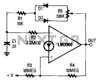
The circuit integrates a charging mechanism through Rl/Dl and the upper half of R5, while discharging occurs via R1/D2 and the lower half of R5. The duty cycle is adjustable within a range of 1:10 to 10:1 through the...
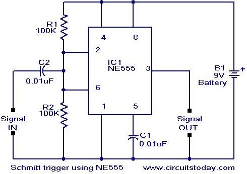
In addition to its timing functions, the two comparators of the 555 timer can be utilized independently for various applications. One such application is a Schmitt Trigger. The inputs of the two comparators (pin 2 and pin 6) are...
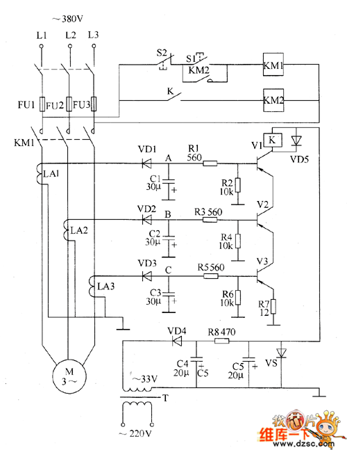
The motor protection circuit consists of a power supply circuit, a current detection circuit, and a protection control circuit, as depicted in the accompanying diagram. The power circuit includes a power transformer (T), a rectifier diode (VD4), filter capacitors...
This audio processor circuit utilizes the SSM2045 integrated circuit (IC), specifically designed for electronic music applications, alongside the 741 operational amplifier (op-amp) IC. The audio processor circuit is centered around the SSM2045, which is renowned for its ability to provide...
A recent thrift shopping experience revealed a toy that appears to be suitable for circuit bending. The toy was found without batteries, preventing any testing at the store. It may be beneficial to bring batteries during future visits or...