
12-Bit dac with variable step size

The described circuit utilizes a digital-to-analog converter (DAC) configuration that allows for precise control over the output current and voltage levels. The first DAC, referred to as DAC A, operates with a stable reference current sourced from a 10.24 V reference integrated circuit (IC) and a resistor (R1). The bias cancellation is achieved through the use of resistor R2, which ensures that any offset errors do not affect the output accuracy.
The choice of using only the first four MSB inputs enables the circuit to achieve a specific step size of 0.127 mA. This current is critical as it serves as the reference for the second DAC (DAC B), which has a refined step size of 0.498 µA. The complementary voltage outputs facilitate unipolar output configurations, and the design allows for an output voltage swing of approximately ±10.2 V when resistors R3 and R4 are set at 10 kΩ. The step size for the output voltage is approximately 5 mV per least significant bit (LSB), providing sufficient resolution for various applications.
In scenarios where a low-impedance output is necessary, the addition of an operational amplifier at the output stage is recommended. This amplifier can be configured to provide a bipolar output that is symmetrical about ground, contingent upon matching resistors R5 and R6 to a tolerance of 0.05%. The inclusion of an offset null feature is essential to enhance the accuracy of the output, ensuring that any inherent offsets are compensated effectively.
The circuit design also allows for flexibility in configuring the DACs. By selecting lower-order address lines for DAC A, it is possible to achieve a smaller step size and a reduced full-scale output. This capability is particularly useful in applications requiring fine-tuning of output levels. Additionally, manipulating unused high-order bits to either a high or low state can adjust the relative positioning of the full-scale output, providing further customization for specific operational requirements. This design approach ensures that the circuit can be tailored to meet a wide range of performance criteria while maintaining high accuracy and stability.The step size of the converter is variable by selection of the high order data bits. The first DAC, A, has a stable reference current supplied via the 10.24 V reference IC and Rl. R2 provides bias cancellation. As shown, only the first 4 MSB inputs are used, giving a step size of 225/256 2.048/16 = 0.127 mA. This current supplies the reference for DAC whose step size is then 0.1275/256 = 0.498 µ. Complementary voltage outputs are available for unipolar output and using R3 - R4 = 10, Vout is ± 10.2 V approximately, with a step size (1 LSB) of approximately 5 mV. If desired an op amp can be added to the output to provide a low impedance output with bipolar output symmetrical about ground, if R5 = R6 within 0.05%.
Note that offset null is required, and all resistors except R2 and R3 should be 1% high stability types. By using lower order address lines than illustrated for DAC A, a smaller step size (and therefore full-scale output) can be obtained.
Unused high order bits can be manipulated high or low to change the relative position of the full-scale output.
Related Circuits
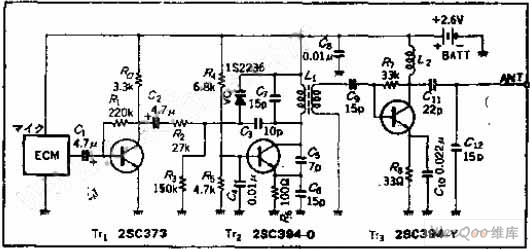
The circuit functions as a frequency modulation (FM) transmitter that operates within the 76 to 90 MHz FM radio band, commonly referred to as a wireless microphone. It receives signals through an FM radio receiver. The circuit is capable...

This circuit utilizes a single potentiometer to control a frequency range from 300 Hz to 3000 Hz. A FET operational amplifier is employed at stages A1 and A2. The upper frequency limit is dictated by the gain-bandwidth product of...
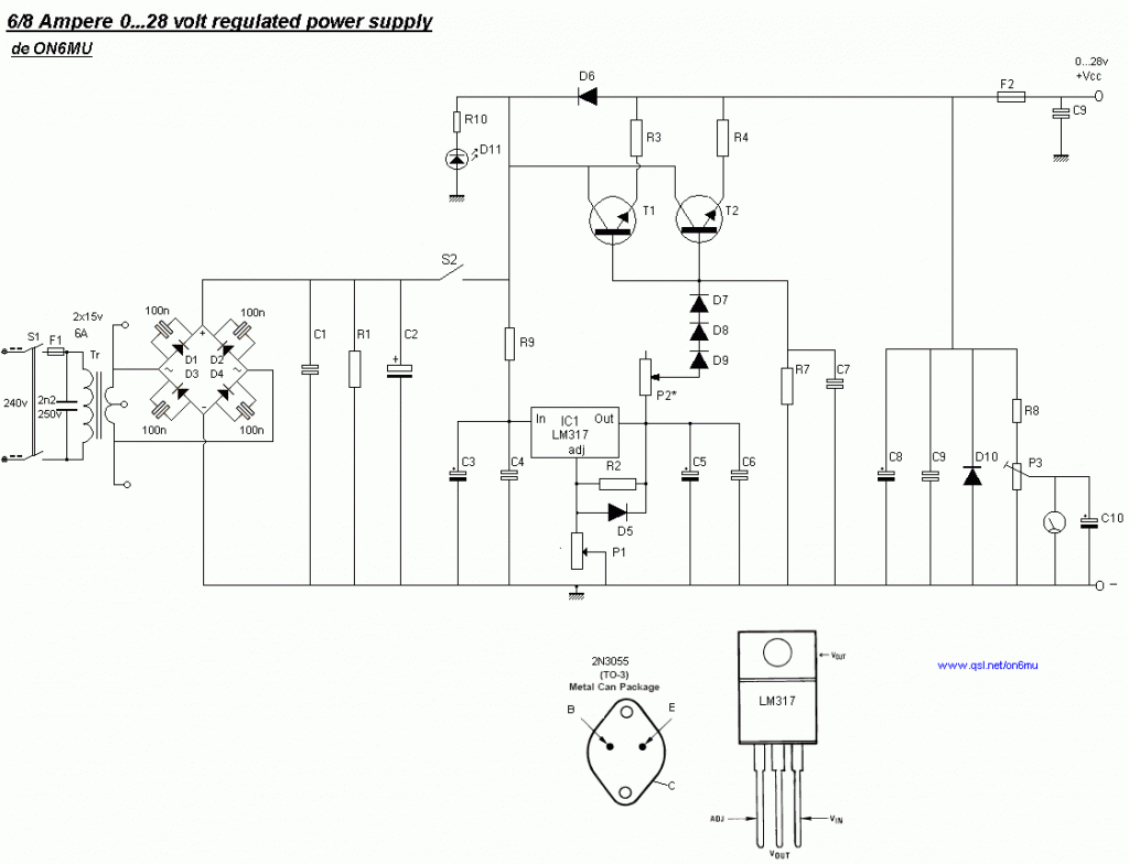
The following diagram is the schematic for a variable power supply that delivers an output voltage ranging from 0 to 28V at a current of 6/8 A. The component part list includes: R1 = 2.2 kΩ, 2.5 Watt; R2...
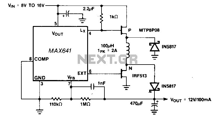
Positive output step-up and step-down converters have a common limitation in that neither can handle input voltages that are both greater than or less than the output. For example, when converting a 12-V sealed lead-acid battery to a regulated...
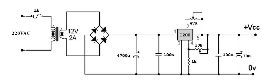
A variable power supply based on the L200 IC, where the output voltage is controlled by a 10K variable resistor. The output voltage ranges from approximately 3 to 15 volts, with a current output ranging from a minimum of...
I found this circuit in my files. I don't know where it came from, but it looks like I photocopied it from somewhere years ago. I have been told that it came from "The Robot Builder's Bonanza", by Gordan...