
12V 40A Switching Power Supply
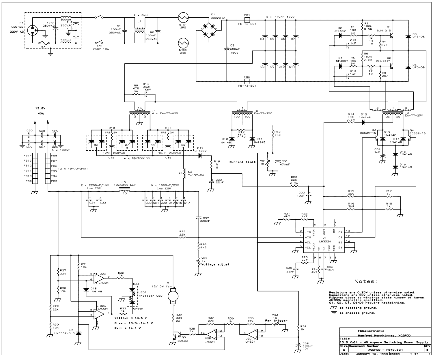
The described circuit is a low-frequency half-bridge converter designed to minimize RF noise while maintaining efficient power conversion. The switching frequency is set at 25 kHz, allowing for effective filtering of RF noise generated during operation. The circuit utilizes bipolar transistors as the primary switching elements due to their lower conduction losses, despite their slower switching speed compared to MOSFETs.
Power is introduced through a CEE-22 connector, which includes a fuse and EMI filtering to protect the circuit from electrical noise. The 2-pole power switch allows for safe operation, while the common-mode noise filter (C1, L1, C2) further reduces interference. Inrush current is limited by two NTC resistors, ensuring smooth startup.
A bridge rectifier converts AC input to DC, charging a large electrolytic capacitor (C3) rated for 300VDC. The power oscillator is made up of two transistors (Q1, Q2) and their associated components, along with a feedback and control transformer (T3) to maintain regulation. The current sensor (T2 and related components) monitors primary current to ensure safe operation.
The output stage includes a power transformer (T1) that generates a square wave approximately 20V, which is rectified by Schottky diodes (D6..9). The output filter comprises a toroidal inductor (L2) and a bank of electrolytic capacitors, providing a stable 13.8V output. Additional components (L3, C23..24) are included for ripple reduction, ensuring a clean output voltage.
The circuit is designed to operate efficiently across varying load conditions. At medium to high loads, the duty cycle is approximately 70%, allowing for a consistent output voltage. The behavior of the inductor (L2) is crucial, as it regulates current flow based on the load, maintaining a ripple current that promotes capacitor longevity.
Feedback and control are managed through the 3524 IC (U1), which integrates multiple functionalities including voltage reference, oscillator, and error amplifier. The output voltage and current levels are continuously monitored, with a PID control loop established using components such as C37, C35, and R23 to ensure stability and responsiveness.
The design includes provisions for soft starting and transient response optimization, preventing overshoot during startup. The cooling system is efficiently managed through a fan controlled by a Schmitt trigger, ensuring the power supply remains cool and operates quietly.
Overall, this half-bridge converter design exemplifies a robust solution for power supply applications, balancing performance, reliability, and longevity.The present trend is to use ever higher frequencies. But by doing so it becomes more difficult to filter out the RF noise inevitably generated by the switching. So I decided to stay at a low switching frequency of only 25 kHz for the full cycle, which due to the frequency doubling effect of the rectifiers results in 50 kHz on the output filter.
For the main switching elements, bipolar transistors or MOSFETs can be used. Bipolars have lower conduction losses, while MOSFETs switch faster. As in this design I wanted to keep the RF noise at an absolute minimum, very fast switching was not desired, so I used bipolar transistors. But these tend to become too slow if the driving is heavier than necessary. The half bridge converter is best controlled by pulse width modulation. There are several ICs available for this exact purpose. I chose the 3524, which is very simple to use and easy to find. Any 3524 will do the job. It can be an LM3524, SG3524, etc. Line voltage enters through a CEE-22 connector with included fuse and EMI filtering (P1). It is then passed through a 2-pole power switch, and an additional common mode noise filter (C1, L1, C2). Two NTC resistors limit the inrush current. A bridge rectifier delivers the power to a big electrolytic capacitor (C3), which works at the 300VDC level.
The power oscillator is formed by Q1, Q2, the components near them, and the feedback and control transformer (T3). T2 and the associated components act as a primary current sensor. T1 is the power transformer, delivering about 20 V square wave to the Schottky rectifiers (D6..9). A toroidal inductor (L2) and a six-pack of low equivalent series resistance electrolytic capacitors form the main filter, while L3 and C23..24 are just there for additional ripple reduction.
The 13.8V is delivered to the output through a string of ferrite beads with some small decoupling capacitors mounted directly on the output terminals. During operation at medium to high load, the duty cycle is about 70%. That means that at the cathodes of the Schottky rectifiers you will have a square wave that stays at about 20V for some 14æs, and then slightly below ground level for 6us.
L2, which has its other end at nearly constant 13.8V, will therefore see about 6V for 14us, followed by -14V for the rest of the time. Given its inductance of about 20uH, the current in L2 will increase by about 4A during each conduction cycle, and decrease by that same amount during rest time.
As long as the current drawn from the power supply is more than 2A, the current in L2 will never stop completely. For example, if 20A are drawn, the current in L2 will vary between about 18 and 22A. As the ripple current stays basically constant while operating at up to the maximum current of the power supply, the filter capacitors C17 to C22 are never exposed to more than about 1.5A RMS total ripple current, assuring them a very long lifetime.
This is an advantage over some other types of switching power supplies, in which the ripple current is much higher, forcing the designer to use more expensive capacitors or to accept reduced lifetime. If the load is less than about 2A, the current flow in L2 is no longer continuous. The duty cycle of the power transistors starts to drop, until at zero load the duty cycle almost becomes zero too.
C37 serves several purposes. For higher frequencies it couples the first filter stage (L2 and C17..22) to the error amplifier, while for lower frequencies and DC the output of the supply is sampled. This is necessary because each filter stage introduces 180 degrees of phase shift at the higher frequencies, so after two stages the phase shift goes through a full 360 degrees, making it impossible to stabilize the control loop without additional circuitry.
But for DC it is good to sample the output, in order to compensate for the voltage drop in L3. So I chose this arrangement. C37 was dimensioned to give the error amplifier a nice PID response, together with R23 and C35. This affords the best possible transient behavior and unconditional stability. In addition, C37 provides some measure of soft starting, so the voltage does not overshoot too much when switching on the power supply. If you have a dual-channel oscilloscope, connect its two channels over the base-emitter junctions of the power transistors.
With the voltage at about 12V, you should see small pulses with opposed phases. As you increase the voltage, suddenly these pulses will disappear. If you want, you can preadjust VR2 by setting your lab power supply to 13.8V and then setting VR2 just to where the pulses disappear. Now it's time to start up the switcher. Remove your lab supply, remove the oscilloscope leads, and connect the beast to the AC line in series with a 60 Watt light bulb.
This technique will avoid most or all damage if something is wrong. Connect a voltmeter to the output, switch on your baby and see what happens! If everything is right, the bulb will light up, then slowly turn off, while the power supply starts up and delivers about 13.8V. Now, connect a load of about 2A to the output. A car bulb is very practical for this. At this load level, probably the bulb in the AC line will glow, while the voltage on the output may be 13.8V or somewhat below.
It depends on the specific current level drawn by your test load. If so far everything is OK, the big moment comes: Remove the bulb from the AC circuit! Now startup of the supply should be fast, and you can connect a heavier load to it. With some load of 2 to 10A connected (the value is uncritical, given the good regulation of this supply), adjust VR2 so that you get exactly 13.8V at the output. R34 and C38 average out the current level over a period of about 2 minutes. U2C amplifies the resulting voltage by a settable amount, and U2D acts as a Schmitt trigger to switch the fan cleanly on and off when the current average crosses the trigger level set by VR3.
R39 limits the speed of the fan to a rather low value which is more than enough to keep the power supply cool. At this low speed the fan produces almost no noise, and can be expected to last longer than its owner..
The control circuit is a 3524 IC (U1), powered from an auxiliary rectifier (D17). The IC contains a voltage reference, oscillator, pulse width modulator, error amplifier, current sense amplifier, flip-flop and driving circuitry. It senses the output voltage and the current level, and through transistors Q3 and Q4 controls the power oscillator.
C37, C35 and R23 are used to implement a full PID (proportional-integral-derivative) response in the control loop. 🔗 External reference
Related Circuits
The first prototype PCB has been completed, but concerns arise regarding the heat generated when utilizing the BMS at maximum power in an ultralight hybrid electric vehicle application. At 30A continuous and 50A burst, nearly 20W of loss occurs....
If you are looking for ICs for a DC to DC converter application, the LM1577/LM2577 ICs are highly recommended as they provide all the necessary power and control functions for step-up conversion. The LM1577 and LM2577 are versatile integrated circuits...
The adaptive adjustable power supply is illustrated in the accompanying figure. The power supply utilizes an LM317 regulator device, and an adaptive switching circuit that automatically adjusts the input voltage based on the output voltage level. This mechanism reduces...
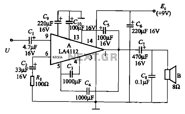
Audio power amplifier circuit utilizing the LA4112 integrated power amplifier along with additional components as shown in the figure. The audio power amplifier circuit based on the LA4112 integrated power amplifier is designed to deliver high-quality audio amplification for various...
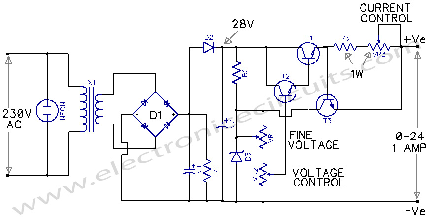
The circuit presented is an economical smooth variable power supply that offers an output range from 0V to 24V. It includes all necessary controls and features protection against short circuits. This variable power supply circuit is designed to provide a...
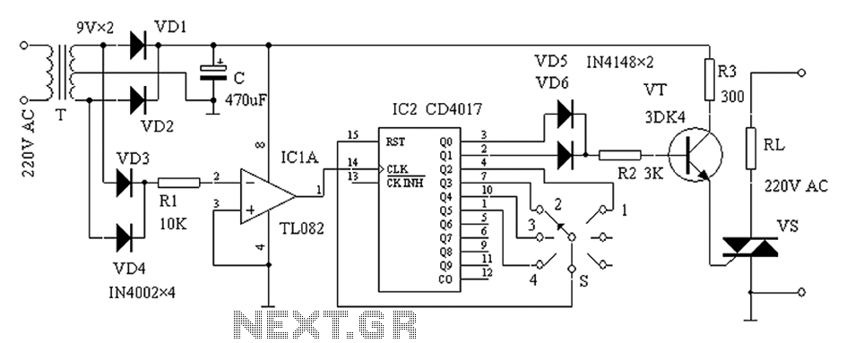
The zero-power regulator circuit is simple, reliable, and functional. It is suitable for various electric power adjustment applications, such as series-wound motor power adjustment. The operational principle of the circuit involves several components, including the power circuit, an AC...
Warning: include(partials/cookie-banner.php): Failed to open stream: Permission denied in /var/www/html/nextgr/view-circuit.php on line 713
Warning: include(): Failed opening 'partials/cookie-banner.php' for inclusion (include_path='.:/usr/share/php') in /var/www/html/nextgr/view-circuit.php on line 713