
170 Watt audio amplifier
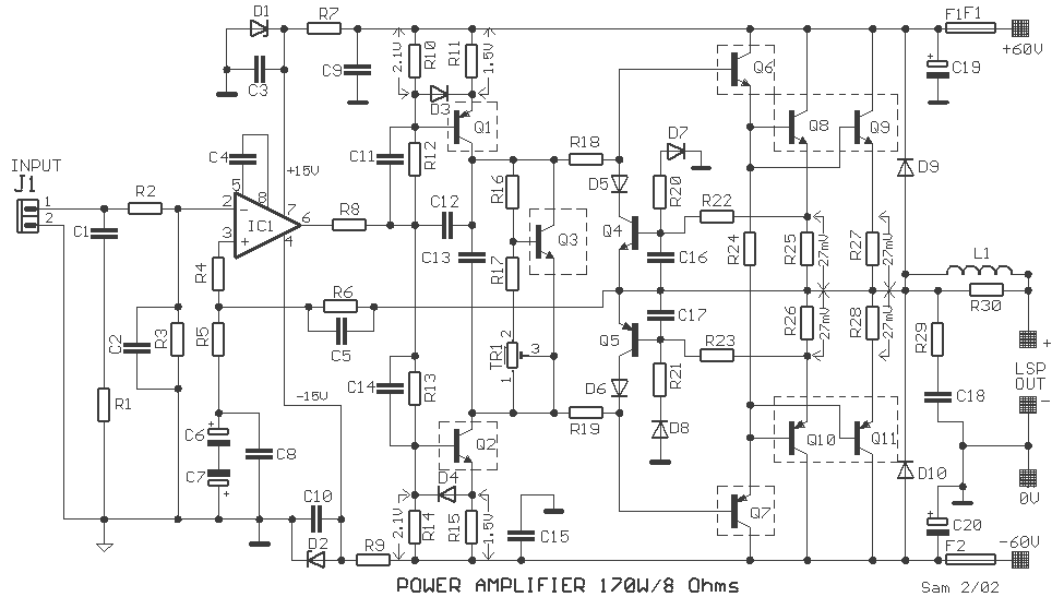
The compensation is achieved through capacitors C4, C5, and C12, while the gain is determined by resistors R5 and R6 (X40). Transistors Q1 and Q2 operate in Class A, with a current of 10mA flowing through them, determined by resistors R10 and R14. The output stage includes power transistors Q8, Q9, Q10, and Q11, which operate in Class AB. This operation is regulated by transistor Q3 and the trimmer TR1, maintaining a quiescent current of 100mA for each output power transistor, corresponding to a voltage drop of 27mV across resistors R25, R26, R27, and R28. To achieve maximum thermal stability, transistors Q1, Q2, Q3, Q6, and Q7 should be mounted on a heatsink along with the power transistors. Diodes D9 and D10 protect the output stage from reverse voltages that may arise from the load. Resistor R29 and capacitor C18 form a classic Boucherot network, which enhances stability at high frequencies. The inductor L1, consisting of 15 turns of wire with a diameter of 1mm, protects the amplifier's output from issues related to capacitive loads. Resistor R30 ensures the unimpeded passage of square pulses due to the inductor's presence.
The construction of the amplifier is manageable for individuals with some experience in the field. However, attention must be paid to the adequate cooling of the power transistors with a suitably sized heatsink, potentially requiring the assistance of a fan, as temperatures tend to rise significantly when the amplifier operates at full power for extended periods, especially with low loads around 4 ohms. The amplifier requires two power supplies, one for each channel. It is advisable to protect the amplifier's output with a protection circuit, as described on the referenced page. This power amplifier design was published in Elektor magazine, December 1995.
SPECIFICATIONS
Input sensitivity: 1 Vrms
Input impedance: 17.8 kΩ
Output Power (0.1% THD): 164W at 8Ω, 275W at 4Ω
Slew Rate: 20V/μs
Signal to Noise ratio: >96dB
THD: <0.004% (1kHz) at 1W (8Ω) and <0.05% (20Hz-20kHz)
IMD (50Hz: 1kHz 4:1): <0.003% at 1W (8Ω) and <0.0035% at 100W (8Ω)
Damping Factor (at 8Ω): >345 at 1kHz and <275 at 20kHz
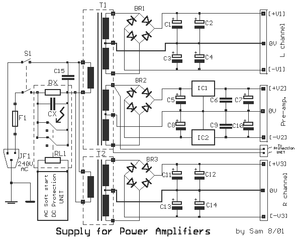
For this power amplifier, a general power supply for power amplifiers is suitable. Due to the amplifier's power requirements, the supply must also have proportional power and high-capacity capacitors. Each power amplifier corresponds to a transformer. A delay protection circuit can be adapted at the transformer input and AC line to ensure a gentle power supply. The cables used should be appropriately rated to handle the voltages and currents required by the amplifier.
Part List
T1: 110-240V @ 2X42.5V 650VA
@[2X15V 1A*]
BR1-3: 400V 35A BRIDGE
C5-8: 2200μF 25V
BR2: 200V 3A BRIDGE
C6-9: 100nF 100V
T2: 110-240V @ 2X42.5V 650VA
C1-2-3-4: 10000μF 100V
C7-10: 47μF 25V
F1: 3.15 AT FUSE
C11-12-13-14: 10000μF 100V
C15: 33nF 630V
RX-CX-RL1
S1: SWITCH 2X2 10A In the drawing he appear simple but powerful power amplifier. His difference with the classic designings, that use differential amplifier in their input, they are that this amplifier it uses a completed the NE5534, in his input. Thus it should we degrade the high voltage of power supply, in ±15V, that needs the IC1. This becomes with the help of R7,9 and Diodes Zener D1,2. In the input exist a High-pass filter C1-R3 and low-pass filter R2-C2, so that is limited the bandwidth of frequencies of unit of entry, in a concrete bandwidth.
The IC1 function as differential amplifier, which the not inverting input (+), work as central node of total feedback. The voltage of feedback from the exit, is applied in the node R4-,R5, via the R6. The compensatory becomes from capacitors C4, C5 and C12, while the gain is appoint by resistors R6, R5, via R6 (X40). Transistors Q1, Q2 works in Class A and the current that elapse from in them is 10mA, (is determined by resistors R10,14).
In the exit exist the power transistors Q8,9,10,11 which work in Class AB, (is regulated by transistor Q3 and the trimmer TR1, in current of calm 100mA, for each one power transistor in the exit, that correspond in fall of voltage 27mV, above in resistors R25,26,27,28). In order to we achieve the biggest possible thermic stability, should transistors Q1,2,3,6,7 be placed above in heatsink, with the power transistors.
The diodes D9-10 protect the output stage, from reverse voltages, that can be created from the load. The R29 and the C18, shape one classic network of Boucherot, which improve the stability in the high frequencies. The inductor L1, (is constituted by 15 coils wire of diameter 1mm), protect the exit of amplifier from problems, because existence of capacitive load.
The R30, ensure the not questioning (because inductor), passage of square pulses. The build of amplifier does not present difficultie for somebody that has a certain experience in the sector. What it should you are careful, is the good refrigeration of power transistors, with one good heatsink, capable dimensions, which probably it needs help from one Fan, because the temperature goes up enough, when the amplifier work in complete power, for big time distance and with low load near in the 4 ohms.
The amplifier will need two power supply, one for each channel. Good it is we protect the exit of amplifier, with a circuit of protection, from what I give in my page. The drawing of this power amplifier, was published in the magazine Elektor 12/95. R1=68Kohm C1=2.2uF 100V MKT Q2=MJE340 R2=2.2Kohm C2=1nF 100V MKT Q3=BD139 R3-6=22Kohm C3-8-9-10-11-14-15=100NF Q4=BC546B R4-22-23=1Kohm C4=33pF 160V polystyrene Q5=BC556B R5-8-10-14=560 ohm C5=47pF 160V polystyrene Q6=MJE15030 R7-9=3.3Kohm 5W C6-7=100uF 63V Q7=MJE15031 R11-15=150 ohm C12=470pF 160V polystyrene Q8-9=MJ15003 R12-13=15Kohm C13=680nF 100V MKT Q10-11=MJ15004 R16=680 ohm C16-17=150nF 100V MKT D1-2=15V 1.5W Z R17=180 ohm C18=33nF 250V MKT D3-4=BAT85 R18-19=10 ohm C19-20=100uF 100V D5-6-7-8=1N4004 R20-21=27Kohm L1= See text D9-10=BY254 R24=56 ohm F1-2=6.3AT FUSE R25-26-27-28=0.27 ohm/ 5W TR1=250 ohms TRIM R29=10 ohm/ 5W IC1=NE5534 R30=2.2 ohm/5W Q1=MJE350 .
SPECIFICATIONS Input sensitivity 1 Vrms Input impedance 17.8 Kohm Output Power (0.1% THD) 164Watt -8 ohms 275Watt- 4 ohms Slew Rate 20V/?s Signal to Noise ratio >96dB THD <0.004% (1KHZ) in 1 Watt -8ohms and <0.05% (20HZ-20KHZ) IMD (50HZ : 1KHZ 4:1) <0.003% in 1Watt 8ohms and <0.0035% in 100Watt 8ohms DAMPING FACTOR (in 8ohm) >345 in 1KHZ and <275 in 20KHZ For the power amplifier, it can be used the general power supply for power amplifiers, that usually I give. Because the power of amplifier the supply it should it has also this proportional power and big capacity of capacitors.
For each power amplifier correspond also a transformer. In the entry of transformers and in line AC, can be adapted the circuit of delay of circuit protection 1, in order that the supply of network become softly. The cables that we will use should be suitable, so that they transport the voltages and the currents, that need the amplifier.
Part List T1=110-240V@ 2X42.5V 650VA @[2X15V 1A*] BR1-3=400V 35A BRIDGE C5-8=2200uF 25V BR2=200V 3A BRIDGE C6-9=100nF 100V T2=110-240V@ 2X42.5V 650VA C1-2-3-4=10000 uF 100V C7-10=47uF 25V F1=3.15 AT FUSE C11-12-13-14=10000 uF 100V C15=33nF 630V RX-CX-RL1 S1= SWITCH 2X2 10A 🔗 External reference
Related Circuits
This circuit is similar to the previous one but employs positive feedback to enhance the amplitude delivered to the speaker. It was derived from a small 5-transistor radio utilizing a 25-ohm speaker. In the previous circuit, the load resistor...
The 30-watt amplifier circuit provides a suitable power boost from an input of 4 watts up to 6 watts. It is designed to operate within the 88-108 MHz FM broadcast band and maintains stability while delivering a clean output...
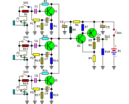
The 3-channel audio mixer is a compact application utilizing transistor amplifiers. This audio mixer operates with a supply voltage of 9V DC, which can be provided by a battery. It is designed specifically for use as a portable amplifier....
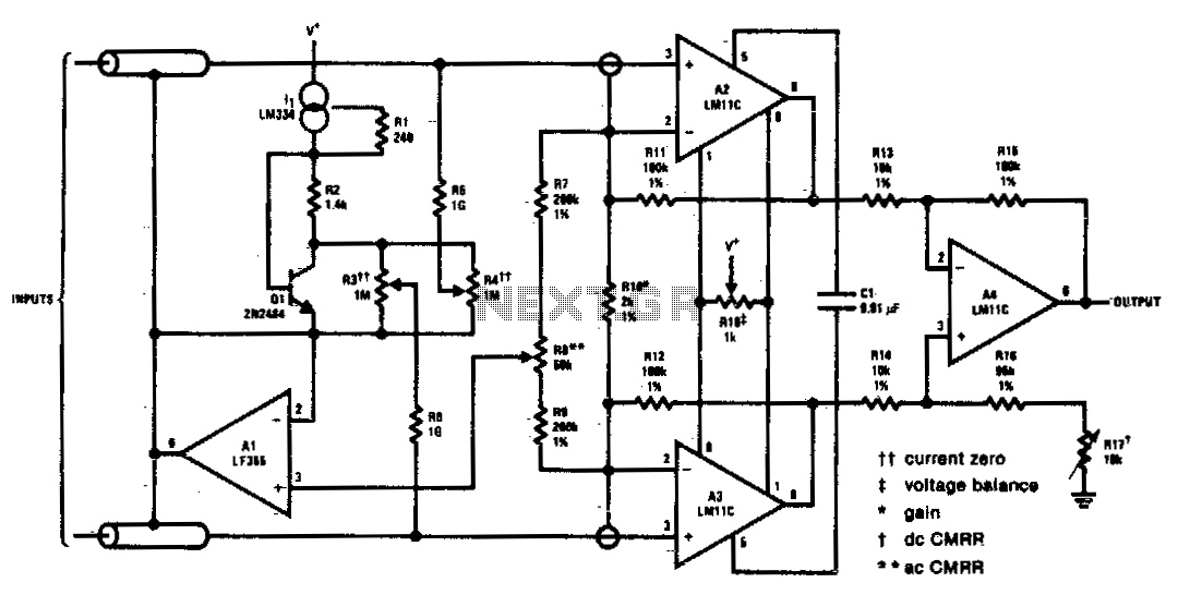
This circuit includes input guarding, cable bootstrapping, and bias current compensation. Differential bandwidth is reduced by Cl, which also makes common-mode rejection less dependent on the matching of input amplifiers. The described circuit features several critical components designed to enhance...
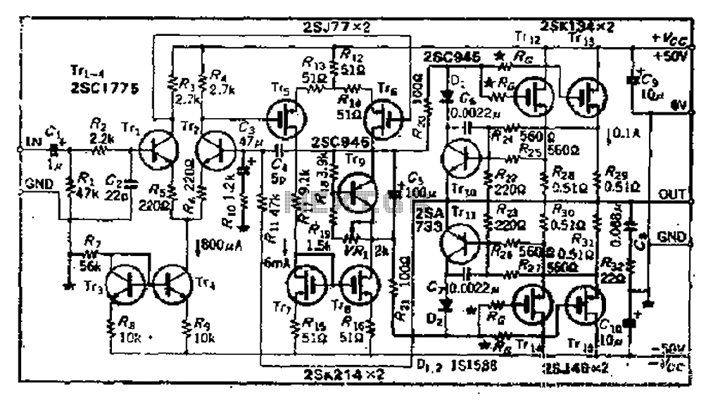
The circuit consists of three identical basic stages, with the second stage featuring a differential output from the power MOSFET, 2SJ77. A current mirror circuit utilizing 2SK214 is implemented. The operating current is 6mA; however, due to the power...
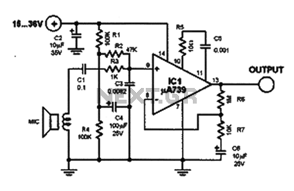
This microphone preamplifier utilizes the low-noise integrated circuit (IC) uA739. It serves as a practical example of designing an effective preamplifier for dynamic microphones. The IC contains two identical integrated preamplifier circuits, with the second preamp functioning in the...