
High gain differential instrumentation amplifier
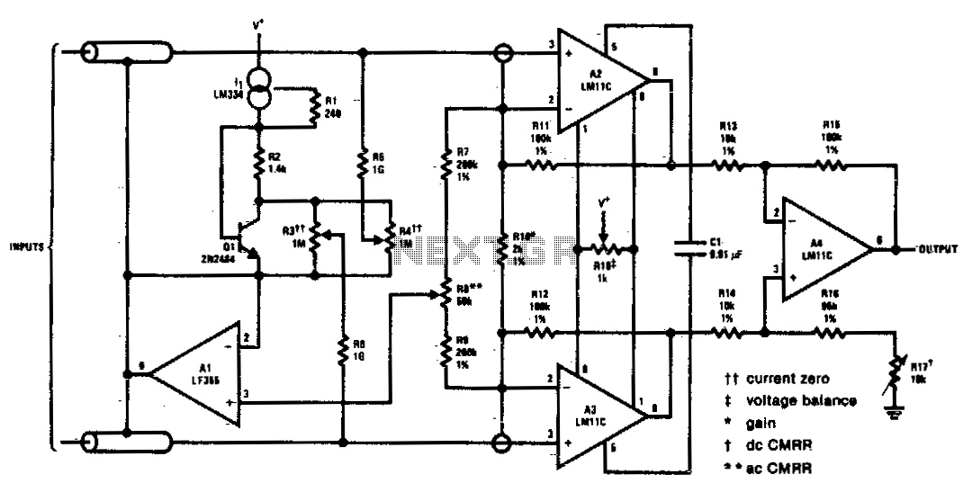
The described circuit features several critical components designed to enhance performance and reliability in electronic applications. Input guarding is implemented to protect the circuit from overvoltage conditions and unwanted noise, ensuring that the input signal remains stable and within the desired range. This is particularly important in sensitive applications where signal integrity is paramount.
Cable bootstrapping is utilized to improve the signal transmission quality by providing a stable reference voltage to the input stage. This technique helps to minimize the effects of cable capacitance and resistance, which can introduce distortions and degrade the overall performance of the circuit.
Bias current compensation is incorporated to address variations in bias currents across different components, particularly in differential amplifier configurations. This compensation ensures that the input stages operate optimally, reducing offset voltages and improving linearity.
The presence of capacitor Cl plays a significant role in the circuit's performance. By reducing differential bandwidth, it effectively limits the frequency response of the circuit, which can be beneficial in certain applications where high-frequency noise needs to be filtered out. Furthermore, the reduced bandwidth contributes to a more favorable common-mode rejection ratio (CMRR). A higher CMRR is achieved as the dependency on the matching of input amplifiers is lessened, allowing for improved noise rejection and enhanced signal fidelity.
Overall, this circuit design emphasizes robustness and precision, making it suitable for various applications in the field of electronics, particularly where signal integrity and noise immunity are critical.This circuit includes input guarding, cable bootstrapping, and bias current compensation Differential bandwidth is reduced by Cl which also makes common-mode rejection less dependent on matching of input amplifiers. 🔗 External reference
Related Circuits
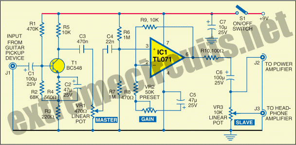
The circuit diagram of a guitar preamplifier is designed to accept any standard guitar pickup. This preamplifier is versatile, featuring two signal outputs. A typical configuration involves a pickup attached to the guitar headstock, where the pickup device consists...
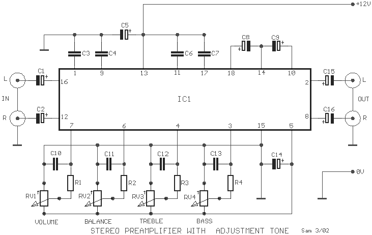
A simple preamplifier circuit is often required, utilizing a few components for ease of construction. This circuit employs an operational amplifier, specifically the Motorola TCA5550, which features a dual amplifier configuration. It provides outputs for adjusting volume, balance, treble,...
The D amplifier utilizes a series fool manifold and can easily be configured as a mono output transformerless (OTL) or output capacitorless (OCL) audio power amplifier. Figure 3-12 illustrates a single-channel power output typical application wiring diagram for OTL....

A simple circuit, High-Pass filter, variable between frequencies 20HZ until 200HZ, useful in a lot of cases elaboration of sound signals. The regulation is achieved with the double potesometer 47K? and the frequency response in his two extreme places,...
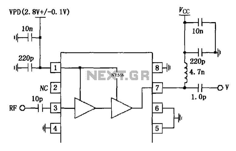
The circuit is constituted by the RF2324 1880MHz internal amplifier collector bias application. A radio frequency (RF) signal enters through input pin 3 and is processed by a preamplifier. The final stage power amplifier output is amplified by 7...
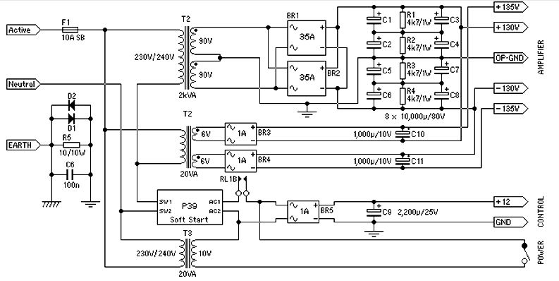
Power supply for a 1500-watt audio power amplifier. This power supply circuit is paired with a high-power audio amplifier rated at 1500 watts. A serious approach is required to design the power supply for the amplifier. First, a step-down...