
2 watt switching power supply
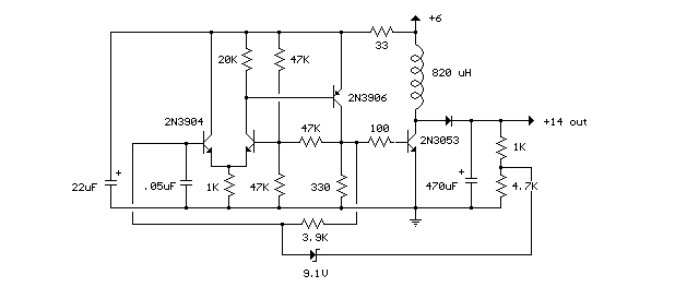
This switching power supply circuit operates by leveraging the principles of inductive energy storage and controlled switching. The Schmitt trigger oscillator generates a square wave signal that toggles the switching transistor, often a MOSFET or BJT, between its on and off states. When the transistor is in the on state, current flows through the inductor, leading to the storage of energy in its magnetic field. The inductor's ability to store energy is primarily determined by its inductance value and the current flowing through it.
Upon switching off the transistor, the inductor releases its stored energy into the load circuit, providing power to the connected device. The output voltage can vary based on the load resistance; as the load resistance decreases, the output voltage tends to increase, and vice versa. The inclusion of a zener diode in the circuit serves a critical role in voltage regulation. It ensures that the output voltage does not exceed a predetermined level (approximately 14 volts) by clamping the voltage and stopping the oscillator when this threshold is reached.
To allow for flexibility in output voltage levels, a voltage divider is implemented, which feeds back a portion of the output voltage to the zener diode. By adjusting the resistor values in this divider network, it is possible to fine-tune the output voltage to meet specific requirements. The design's efficiency, rated at about 80%, is a result of the high-quality inductor used, which minimizes energy losses during the switching process. The circuit's compact nature and high efficiency make it suitable for various applications, including portable devices and low-power electronics.In this small switching power supply, a Schmitt trigger oscillator is used to drive a switching transistor that supplies current to a small inductor. Energy is stored in the inductor while the transistor is on, and released into the load circuit when the transistor switches off.
The output voltage is dependent on the load resistance and is limited by a zener diode that stops the oscillator when the voltage reaches about 14 volts. Higher or lower voltages can be obtained by adjusting the voltage divider that feeds the zener diode.
The efficiency is about 80% using a high Q inductor.. 🔗 External reference
Related Circuits
FGDF-3 is a three-phase low-temperature iron plating power commutation control switch and electronic circuit. The KGDF-3 serves as a low-temperature iron plating power supply device, incorporating the characteristics of a single-phase low-temperature iron plating power supply. This design facilitates...
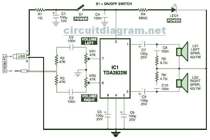
USB Powered Stereo PC Multimedia Speaker Circuit Diagram. This circuit is powered by a 5V DC source obtainable from the USB port of a computer. When the electrical power switch S1 is turned to the "on" position, the 5V...
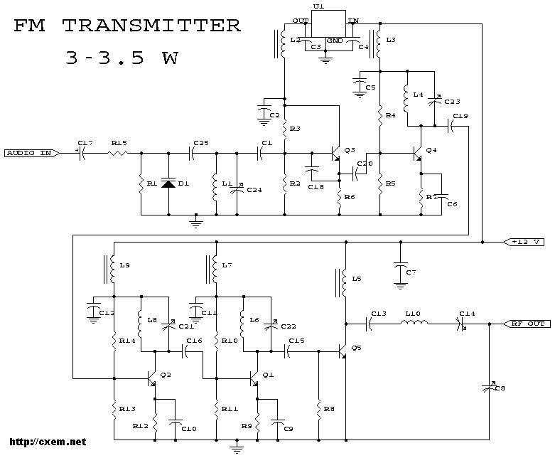
3-3.5 Watt FM Transmitter. This is the schematic for an FM transmitter with 3 to 3.5 W output power that can be used between 90 and 110 MHz. Although the stability is not so bad, a. The 3-3.5 Watt FM...
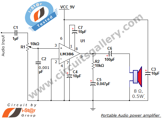
The i-St@r presents a simple mini audio amplifier circuit schematic utilizing the LM386 low voltage audio power amplifier IC. This circuit is designed to power medium-sized speakers from a music player that typically drives only earphones (LM386 headphone). The...
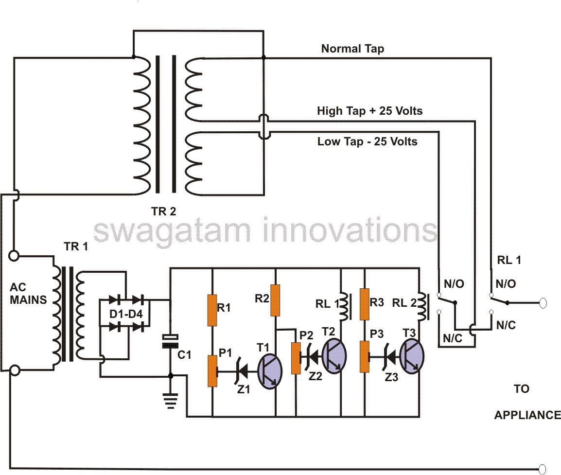
This power stabilizer circuit utilizes one relay to select either the high or low tap from the stabilizer transformer at a specific voltage level. The second relay maintains the normal mains voltage, but when a voltage fluctuation occurs, it...
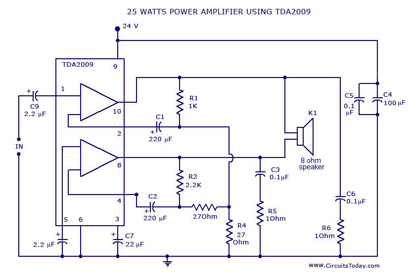
Power amplifier circuit diagram with schematics. This simple audio power amplifier circuit is designed for 25 watts output power using TDA 2009 IC, which has two channels (stereo), 12.5 W for each channel. The described power amplifier circuit utilizes the...