
2400 MHz RF amplifier circuit diagram using PM2107
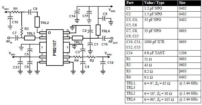
The PM2107 RFIC amplifier is designed specifically for applications within the 2400 MHz ISM band, making it suitable for various wireless communication systems. The two-stage amplifier configuration allows for increased gain and improved linearity, essential for maintaining signal integrity in high-frequency applications. The off-chip matching technique enhances the amplifier's performance by optimizing the input and output impedance, which is critical for maximizing power transfer and minimizing signal reflection.
The power supply of 5 volts is standard for many RF applications, providing a balance between performance and power consumption. With the capability to deliver 1 watt of saturated output power, the PM2107 is well-suited for applications requiring robust signal transmission, such as in wireless sensor networks, Bluetooth devices, and other short-range communication systems.
Grounding plays a vital role in the performance of the amplifier. Pin 1, which is the primary input pin, must be grounded through a transmission line to achieve the desired input matching. This approach helps in minimizing reflections and enhancing stability within the operational bandwidth. The other ground pins (5, 6, 10) are also connected to ground through low inductance paths to ensure that the amplifier operates efficiently and reduces the risk of oscillations.
The input matching network, formed by TRL1, TRL2, C8, and R3, is designed to create a lossy match that effectively manages the impedance seen by the amplifier. This configuration allows for better signal handling and contributes to the overall stability of the amplifier. TRL2, in particular, is critical as it provides ground isolation between the two amplifier stages, which is essential for preventing unwanted feedback and ensuring that each stage operates independently.
The output matching network, consisting of TRL3, C1, and C2, is designed to optimize the output impedance of the amplifier to match the load, ensuring maximum power transfer. This network is crucial for maintaining the efficiency of the amplifier and minimizing distortions that could affect the quality of the transmitted signal.
Overall, the PM2107 RFIC amplifier is engineered for high-performance applications within the 2400 MHz ISM band, with careful attention given to grounding, matching networks, and stability, ensuring reliable operation in various wireless communication scenarios.applications in the 2400 MHz ISM band. This two stage RFIC amplifier is off-chip matched to provide optimum performance for a variety of applications. Operating from a 5 volt supply, the PM2107 can produce 1 watt of saturated output power with 45% typical efficiency.
The inductance to the microstrip ground plane should be as low as possible in gro unding these pins. Pin 1 should be grounded through a transmission line to achieve the required input match and improve inband stability. The other ground pins (5, 6, 10) should also be connected to ground through a low inductance path. A lossy input match is formed by TRL1, TRL2, C8, and R3. TRL2 provides ground isolation between the two stages to improve stability. The output matching network consists of TRL3, C1, and C2. 🔗 External reference
Related Circuits
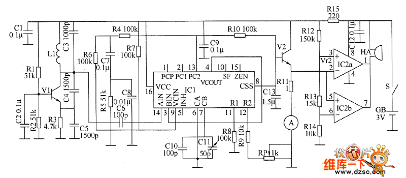
The metal detector circuit consists of a probe oscillator, a PLL (phase-locked loop) circuit, and an audio alarm circuit. The probe oscillator includes a detection coil (L), transistor (V1), and several resistors (R1 to R3) and capacitors (C1 to...
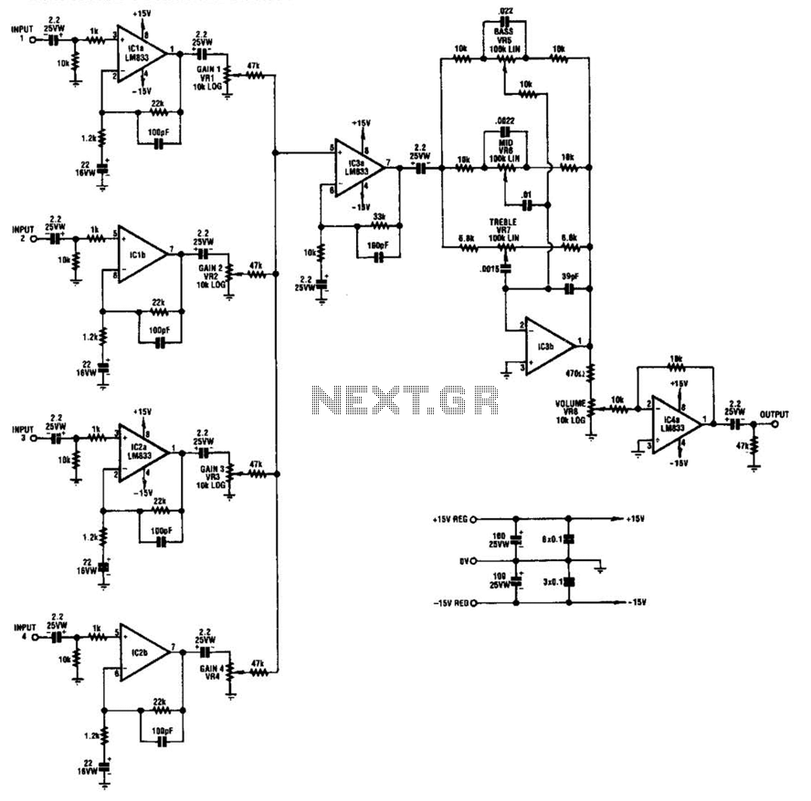
IC1-a, IC1-b, IC2-a, and IC2-b all operate with a gain of approximately 19. Their outputs are combined through level-control potentiometers, and the resulting signal is amplified by IC3-a before being sent to the tone-control stage IC3-b. Finally, the output...
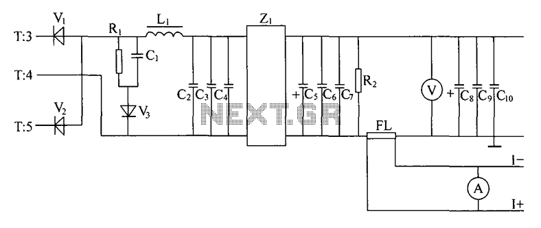
Alternating positive and negative voltage pulses from the secondary winding of a high-frequency transformer (T) are full-wave rectified by high-frequency switching diodes (V1, V2). The output is then filtered through inductors (L1) and capacitors (C2, C3, C4) which form...
This is a simplified schematic for the Solar Lifeforce. The design eliminates the expression/CV output features and the toggle for the buffer, making it a straightforward circuit. It may benefit from adding small capacitors between R5 and ground, as...
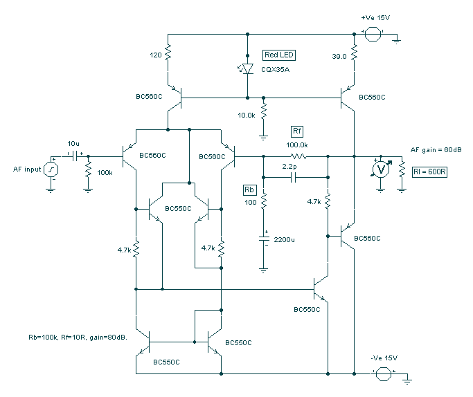
The circuit was submitted by an individual from Newtownabbey, Northern Ireland. It has an exceptionally fast high frequency response, as demonstrated by applying a 100kHz squarewave to the input. All graphs were produced using Tina Pro. The circuit in question...
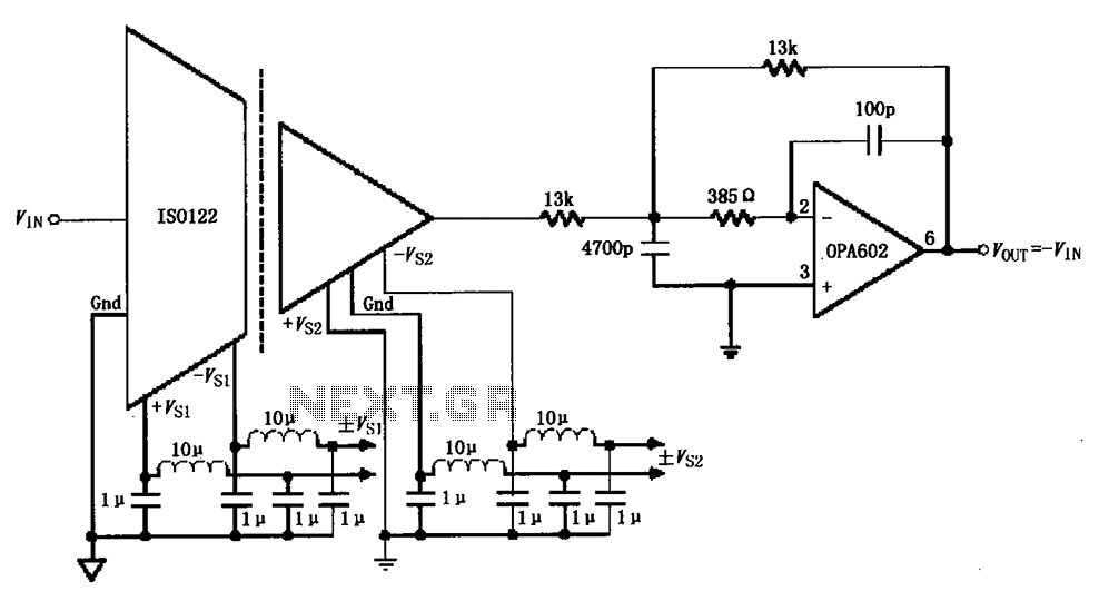
The ISO122/124-type filter circuit is designed to address noise suppression from the DC/DC converter. The internal oscillator frequency of the ISO122/124 modem is set to 500 kHz. The circuit employs inductors and capacitors for filtering to mitigate any beat...
Warning: include(partials/cookie-banner.php): Failed to open stream: Permission denied in /var/www/html/nextgr/view-circuit.php on line 713
Warning: include(): Failed opening 'partials/cookie-banner.php' for inclusion (include_path='.:/usr/share/php') in /var/www/html/nextgr/view-circuit.php on line 713