
DZW75-48 50 50II high-frequency rectifier circuit

The circuit operates by converting the alternating voltage generated in the secondary of the high-frequency transformer into a usable direct current. The high-frequency switching diodes (V1, V2) are essential for efficient rectification, allowing for rapid switching and minimal losses. The L-type filter, consisting of the inductor (L1) and capacitors (C2, C3, C4), is designed to smooth the rectified output while attenuating high-frequency noise that may interfere with sensitive electronic components.
The output voltage regulation is achieved through careful manipulation of the pulse width, which is controlled by the switching frequency of the transformer. This feature allows the circuit to adapt to varying load conditions, maintaining a consistent 48V output regardless of fluctuations in input or load. The inclusion of a voltmeter provides real-time feedback on the output voltage, ensuring that any deviations from the desired level can be monitored and corrected.
R2, the bleeder resistor, plays a critical role in discharging capacitors when the circuit is powered down, preventing potential hazards from stored energy. The shunt (FL) facilitates accurate current measurements, providing essential data for the current limiting and sharing circuits. This ensures that the output current remains within safe operating limits, protecting both the power supply and connected loads.
The RCD snubber circuit, composed of R1, C1, and V3, is strategically placed to mitigate voltage spikes that can occur during the switching process. This protection is vital for enhancing the longevity and reliability of the diodes and other circuit components, preventing damage from transient voltage events. Overall, the design emphasizes efficiency, stability, and safety in delivering a regulated DC output.Alternating positive and negative voltage pulses of high-frequency transformer T secondary sensing, full-wave rectified by the rectifier High frequency switching diodes V1, V2 composition, and then after L1 inductors and capacitors C2, C3, C4 consisting of L-type filter and power supply Z1 smoothing filters at the output of high-frequency noise to get in line with the indicator of 48V DC voltage output. Pulse width directly determines the output voltage level. Wide pulse width, high output voltage, narrow pulse width, output voltage is low. And picked up at the output a voltage meter to measure the output DC voltage display. R2 is a bleeder resistor, FL for the shunt, a current meter is connected across both ends FL measurements show that the output current value rectifier, FL voltage across the current sampling value is also used as an output signal to the voltage regulator and current limiting, current sharing circuit.
R1, C1 and V3 composition RCD snubber circuit to absorb the secondary voltage overshoot.
Related Circuits
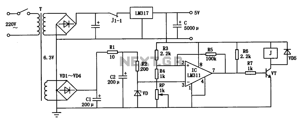
The circuit depicted can be utilized to operate at a voltage of +5V for Single Board Computer (SBC) power, preventing damage caused by over-voltage from the power supply throughout the SBC. This circuit serves as a protective mechanism for Single...
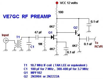
This is a simple VE7GC Popcorn RF preamplifier designed by Dick Pattinson. The circuit features a single tuned circuit at the input stage, allowing direct connection to a mixer or product detector in a straightforward receiver project. Adjustable RF...

A bidirectional H-bridge DC motor control circuit is illustrated. The circuit utilizes the L298 integrated circuit from ST Microelectronics. The L298 is a dual full-bridge driver that supports a wide operating voltage range and can manage load currents up...
Assistance is required regarding the circuits provided below. The focus is on an ultrasonic receiver circuit that utilizes two ultrasonic components. The ultrasonic receiver circuit is designed to detect ultrasonic waves, typically in the frequency range of 20 kHz to...
This is the circuit diagram of a line follower/line tracker robot. The circuit is derived from tutorial documentation, which can be downloaded at the end of this article. The line follower robot utilizes eight proximity sensor modules. Each sensor...
The gain of the single-stage virtual earth amplifier IC1 is determined by the drain-source resistance of the field-effect transistor (FET). Resistors R1, R2, and R3 linearize the FET's voltage-current characteristic. A control voltage is derived from the output signal...