
2M Fet Power Amplifier Circuit

The described amplifier utilizes a power MOSFET as its primary amplification component, which is capable of handling significant power levels while maintaining efficiency. The 2-W output power is suitable for handheld transceivers, allowing for effective communication over short distances. The amplifier's design is optimized for operation on the 2-meter band, commonly used in amateur radio, which enhances its usability for hobbyists and professionals alike.
To facilitate the transition between transmitting and receiving modes, a transmission-line RF switch is integrated into the circuit. This type of switch is advantageous due to its low insertion loss and high isolation characteristics, which are crucial for maintaining signal integrity during operation. The RF switch effectively routes the signal from the amplifier to the antenna during transmission and connects the receiver to the antenna during reception.
The overall design of the amplifier circuit includes necessary biasing components for the MOSFET, ensuring that it operates within its optimal range. The layout should minimize parasitic inductances and capacitances to enhance performance and reliability. Proper heat dissipation measures, such as heat sinks or thermal pads, are also essential, given the power levels involved.
In summary, this amplifier design combines the efficiency of a power MOSFET with the reliability of a transmission-line RF switch, making it suitable for applications requiring moderate power output on the 2-meter band. The circuit's design considerations play a critical role in achieving the desired performance characteristics while ensuring robust operation in various conditions. Using a power MOSFET, this amplifier can boast a 2-W handie-talkie power level to around 10 W on 2 meters. A transmission-line RF switch is used for T/R switching. 🔗 External reference
Related Circuits
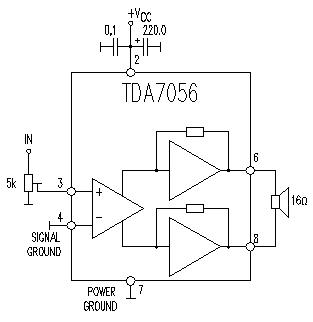
This TDA7056 power audio amplifier circuit diagram project is designed to deliver a maximum output power of 1 watt into an 8-ohm load when powered by a 6-volt supply, or a maximum output power of 3 watts into a...
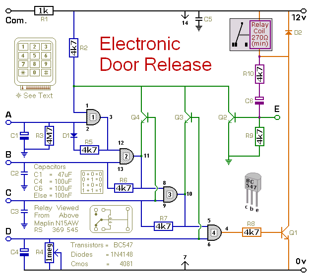
This circuit is designed to operate an electrical door-release mechanism, but it can also be utilized for other applications. When the user enters a four-digit code of their choice, the relay will energize for a preset time period. The...
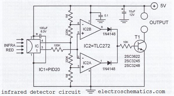
This infrared detector circuit utilizes a passive infrared detector component, PID20, which converts heat radiation into electrical impulses. The output voltage of the PID20 increases when an object approaches, provided that the object is warmer than the surrounding environment....
This circuit measures the distance covered during a walk. The hardware is housed in a small box that can be placed in a pocket, and the display is designed as follows: the leftmost display D2 (the most significant digit)...
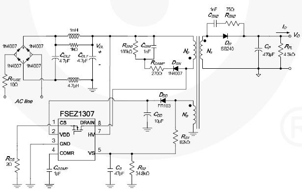
This cell phone charger circuit diagram electronic project is based on the FSEZ1307 third-generation primary side regulation (PSR) PWM controller integrated circuit. The FSEZ1307 cell phone charger can be used for battery charger applications for devices such as cellular...

Figure 1 illustrates an economical and straightforward Gate Alarm designed to operate using a small universal AC-DC power supply. IC1a functions as a fast oscillator, while IC1b serves as a slow oscillator. These two oscillators are integrated through IC1c...