
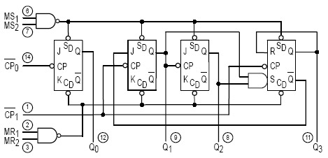
4013 datasheet

The 4013 dual D-type flip-flop serves as a fundamental building block in digital electronics, capable of storing one bit of data. The device operates on the principle of edge-triggered operation, meaning that the output state changes in response to the clock input's rising or falling edge, depending on the specific configuration.
Each flip-flop consists of two main inputs: the data input (D) and the clock input (CLK). The output (Q) reflects the state of the data input (D) at the moment the clock signal transitions, while the complementary output (Q') provides the inverse state. Additionally, the flip-flop includes asynchronous set (SET) and reset (RESET) inputs, allowing for immediate control over the output states regardless of the clock signal. When the SET input is activated, the Q output is set to high (logic 1), while the Q' output goes low (logic 0). Conversely, activating the RESET input forces the Q output to low (logic 0) and the Q' output to high (logic 1).
The 4013 flip-flop is commonly used in various applications, including data storage, frequency division, and as a building block for more complex digital circuits such as counters and shift registers. The CMOS technology employed in the construction of the 4013 ensures low power consumption and high noise immunity, making it suitable for battery-operated devices and portable electronics.
The pin configuration typically includes VDD (power supply), GND (ground), and the respective inputs and outputs for both flip-flops. The device operates within a specified voltage range, typically from 3V to 15V, providing flexibility in design for different logic levels.
In summary, the 4013 dual D-type flip-flop is a versatile and essential component in digital circuit design, enabling reliable data storage and manipulation while ensuring efficient performance in a wide range of electronic applications.4013 dual D-type flip-flop is a monolithic complementary MOS (CMOS) integrated circuit constructed with N- and P- channel enhacement mode transistors. Each.. 🔗 External reference
Related Circuits
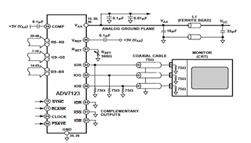
This digital-to-analog converter (DAC) integrated circuit is designed for optimal noise performance, minimizing both radiated and conducted noise. A recommended connection diagram for the ADV7123 is depicted in the following schematic diagram. According to the ADV7123 datasheet, this device...
The multifunction circuit primarily refers to its capability to operate in three modes: "delayed pull," "time release," and "delayed cycle." The term "delay" indicates that the relay is energized after a predetermined time; however, the relay does not activate...
A four-button RF remote control is designed to independently turn ON and OFF four different devices. Each of the four outputs can be configured to operate independently in either toggle or momentary mode. The outputs are buffered using BC549...
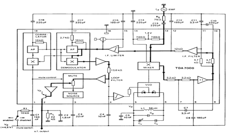
The TDA7000 is an integrated circuit (IC) designed for FM portable radios, featuring a Frequency-Locked Loop (FLL) system with an intermediate frequency of 70 kHz. It incorporates several functions, including an RF input stage, mixer, local oscillator, IF demodulator,...
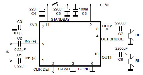
The car radio application utilizes a Class AB Audio Power Amplifier, typically featuring the TDA7360 IC. This amplifier provides 22W output in either bridge or stereo configuration and includes several beneficial features such as a minimal requirement for external...
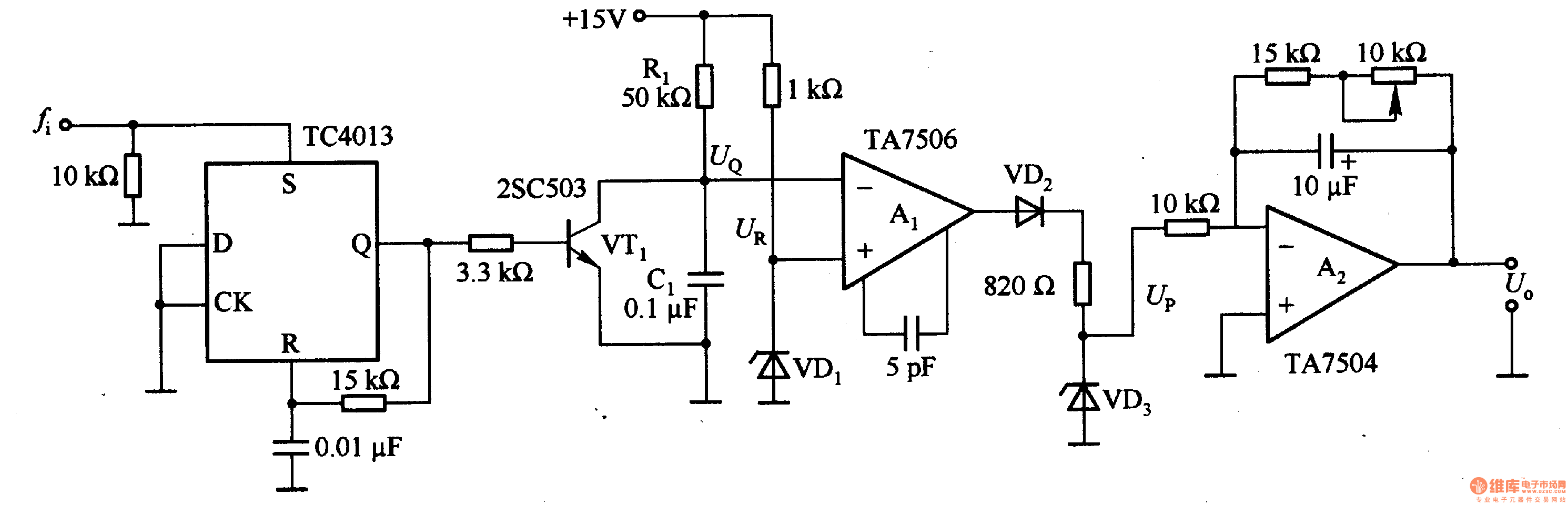
This circuit can convert an input frequency ranging from 0 to 100 Hz into an output voltage of 0 to 10 V. It utilizes the TC4013 monostable multivibrator to shape and amplify the input pulse, which has a width...