
4081 AND gates

The described circuit employs a combination of CMOS technology and digital logic to create a reliable and efficient combination lock system. The design emphasizes the importance of ensuring that all inputs are properly terminated to prevent floating states, which can lead to unpredictable behavior in digital circuits. The inclusion of pull-down resistors serves to ensure that the inputs are pulled to a defined LOW state when not actively driven HIGH.
The use of a transistor switch indicator circuit is a strategic choice to prevent loading on the output of the gate, which can affect the performance of the circuit. This is particularly critical in CMOS applications where gate capacitance can lead to increased power consumption and slower switching times if not managed properly.
Decoupling capacitors play a vital role in stabilizing the power supply by filtering out high-frequency noise and voltage spikes that may occur during operation. The recommended values of 47 µF or 100 µF are suitable for most applications, providing a buffer that helps maintain a stable voltage level across the circuit.
In the context of the bistable operation, the circuit demonstrates a clear latching mechanism, allowing for stable output states until a specific action is taken (pressing the SET or RESET buttons). This behavior is essential for applications such as combination locks, where the state must be maintained until a reset is intentionally performed.
The sequential operation of the four AND gates, along with the parallel configuration of the unselected switches, allows for a flexible and user-friendly interface. This design choice enables multiple reset options, enhancing the usability of the lock system.
The necessity of capacitors to eliminate glitches underscores the importance of careful circuit design, particularly in digital applications where timing and signal integrity are crucial. The combination of capacitors at various values (1 µF, 100 nF, and 10 nF) ensures that the circuit remains robust against transient disturbances that could lead to erroneous resets.
Overall, this combination lock circuit exemplifies effective use of CMOS technology and digital logic principles to achieve a practical and reliable solution for security applications. The ability to generate a large number of combinations with a simple 10-switch keyboard makes it a versatile option for various locking mechanisms. The final output interface can easily integrate with solenoid lock systems or other devices, providing a straightforward implementation for locking solutions.The inputs of the gate must be connected, either to LOW or to HIGH, and must not be left open circuit. This is the function of the input switches with their pull-down resistors. To avoid loading the output of the gate, a transistor switch indicator circuit should be used. It is good practice with CMOS circuits to insert a decoupling capacitor, 47 µF or 100 µF, across the power supply. (This helps to prevent the transfer of spikes along the power supply rails. ) In the prototype circuit, it is not essential to make connections to the unused gates. However, in any final circuit, all unused CMOS inputs must be connected either to HIGH or to LOW. Make it an absolute rule that CMOS inputs are never left open circuit. Click on the diagram and confirm the latching action of this circuit. When you click the SET button, the output goes HIGH and stays HIGH. This is one of the stable states of the bistable. Nothing further happens unless you click the RESET button, making the ouput LOW once more. Click the diagram to open a Crocodile Technology © simulation of the circuit. The four AND gates operate in sequence and are connected to the push button switches included in the code. The remaining, unselected, switches are connected in parallel and pressing any one of them RESETS all the AND gate bistables.
With a real circuit using 4081 AND gates, the 1 µF, 100 nF and 10 nF capacitors are found to be necessary to eliminate a `glitch` caused by pressing the next switch in the sequence. Without the capacitors, pressing the next switch can RESET the previous AND gate. With the capacitors, the circuit operates reliably. This is an unusual way to make a combination lock but the components needed are cheap and easily available.
With no repeat digits, a 10-switch keyboard will give 10x9x8x7=5040 different combinations. The output of the final AND gate can be connected to a solenoid lock system, or other output device. 🔗 External reference
Related Circuits
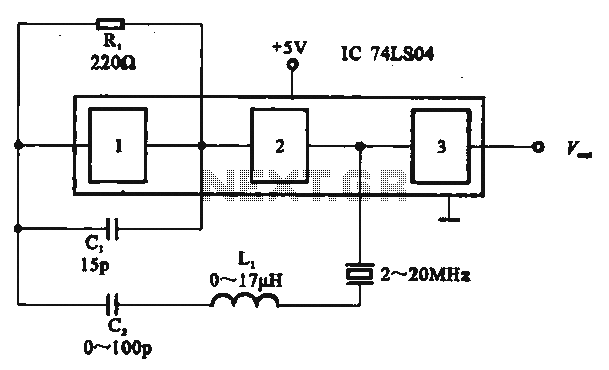
The circuit includes several gates arranged as a crystal oscillator circuit. Figure (A) illustrates a crystal oscillator circuit operating at 1 MHz, while Figure (B) depicts a 20 MHz crystal oscillator circuit. Figure (C) represents a variable crystal oscillator...
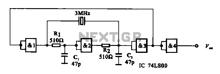
A crystal oscillator circuit is composed of several gates. Figure (A) illustrates a crystal oscillator circuit operating at 1 MHz, while Figure (B) depicts a 20 MHz crystal oscillator circuit. Figure (C) represents a variable crystal oscillator circuit with...
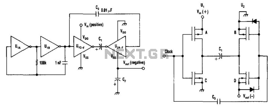
This circuit utilizes a charge pump and an oscillator operating at 7 kHz. When the clock signal is high, capacitors C and D are activated, grounding the positive side of capacitor CI and providing a negative voltage at the...
The bedside door fixture delay circuit features a straightforward design and offers cost-effectiveness. It is constructed using a hex inverter CD4069. The bedside door fixture delay circuit employs the hex inverter CD4069, which is a versatile integrated circuit (IC) commonly...
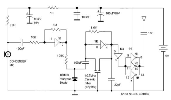
Logic Gates FM Transmitter Circuit Electronic Circuit Schematic Wiring Diagram. The FM transmitter circuit utilizing logic gates is a fundamental electronic design that operates by modulating a carrier frequency with an audio signal. This circuit typically consists of various logic...
There are integrated circuits that contain AND, OR, and NOT gates. The inquiry revolves around the existence of a single chip that encompasses all the required logic gates. If such a chip does not exist, specific alternatives should be...