
51 one-chip computer ADC0804 analog to digital converter studies

The ADC0804 is an 8-bit successive approximation analog-to-digital converter (ADC) that interfaces seamlessly with microcontrollers. It converts an analog voltage signal into a digital representation that can be processed by digital systems. The left-handed configuration of the ADC0804 indicates that the input signals are processed from the left side of the chip, while the right-handed configuration of the 74HC573 latch indicates that the output signals are managed from the right side. The 74HC573 is a high-speed, octal D-type latch that captures data on the rising edge of the clock signal, allowing for precise timing and control of the data flow between the ADC and the microcontroller.
In this circuit, the CSAD pin acts as a gatekeeper, ensuring that the ADC0804 is only active when selected by the microcontroller. The RD pin allows the microcontroller to read the converted digital data from the output pins DB0-DB7. The WR pin initiates the conversion process, signaling the ADC to begin sampling the analog input voltage. The INTR pin provides feedback to the microcontroller, indicating when the conversion is complete and the data is ready to be read.
The ground connections, AGND and DGND, are critical for stable operation, ensuring that all components share a common reference voltage. The clock signals provided by CLK R and CLK IN are essential for the timing of the ADC0804's internal processes. The RC oscillating circuit connected to these clock pins generates the necessary clock pulses to synchronize the ADC's operations.
The analog input to the ADC0804 can come from various sources, with the sliding potentiometer being a practical example. As the potentiometer is adjusted, it varies the voltage level fed into the ADC, which is then converted into a digital value. This digital output can be displayed on a nixie tube, providing a visual representation of the analog input in decimal format. The combination of these components allows for a versatile and effective analog-to-digital conversion system suitable for various applications in electronic design.It is ADC0804 to be left-handed, it is 74HC573 latch to be right hand, the latch connected the one-chip computer and has not drawn at the same time. The pin CSAD of ADC0804 is a chip selection pin because acted as effectively by the low level Hand over 0 hour, we can choose it to work.
RD is that the low level is effective too, it is the read sign al one, WR is that the low level is effective too, can start A/D to begin to be changed when giving 0. INTR is changed and formed One bunch of pins, it is that the low level is effective too, when INTR is 0, represent the end of conversion.
DB0-DB7 is a digital signal output port after changing. AGND and DGND are earthy. CLK R and CLK IN namely 19 and 4 pins Used for, it gives ADC0804 to be pulsing to produce the internal clock Have connected a RC oscillating circuit 6, and 7 port input end of analog signal such as we slip potentiometer on This following procedure carries on the analog to digital converter with the one piece mechanically controlled ADC0804, acts as and twists the potentiometer a slide rheostat on the breadboard When, the digital quantity after the dynamic display A/D in decimal system way of the top three of the nixie tube is changed. The code is as follows: 🔗 External reference
Related Circuits
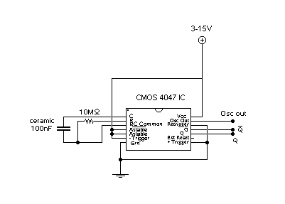
This circuit provides a digital square wave that can be viewed directly or used to drive other circuits. It used the CMOS 4047 Low-Power Monostable/Astable Multivibrator. As used in Tom Duncan's Adventures with Digital Electronics Book, to drive CMOS...
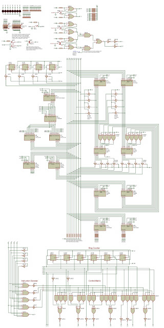
An almost identical recreation of the SAP-1 Simple As Possible microprocessor, as published in "Digital Computer Electronics" by Albert Malvino and Jerald Brown. While the book is out of print, an eBook can be found relatively easily if one...
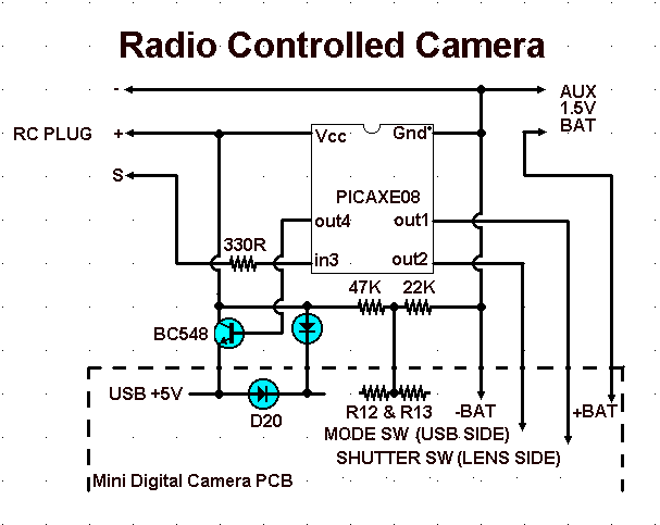
The aim of this project was to get a digital camera into a small electric radio controlled (RC) aeroplane and still have it fly. The aeroplane shown, a park flyer, weighs between 400 and 550 grams depending on the...
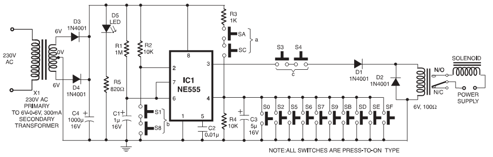
In these circuits, a set of switches (conforming to code) are pressed sequentially within a specified time to unlock the mechanism. In some configurations, custom-built integrated circuits (ICs) are utilized, and positive and negative logic pulses are input in...
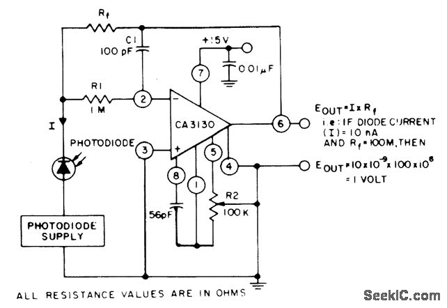
The circuit employs three CA3130 BiMOS operational amplifiers in an application that is sensitive to sub-picoampere input currents. It generates a ground-referenced output voltage that is proportional to the input current flowing through the photodiode. The described circuit utilizes three...
Use microcontrollers to establish serial communication between the AVR-006 kit and a computer. This project utilizes the AVR-006 microcontroller from Circuits-Home. Before developing the program, it is essential to understand the hardware specifications. An example program (in C) for...