
PHOTODIODE CURRENT TO VOLTAGE CONVERTER

The described circuit utilizes three CA3130 BiMOS operational amplifiers, which are specifically designed for high-impedance applications, making them suitable for detecting very low input currents, such as those in the sub-picoampere range. The CA3130 op-amps feature a unique combination of CMOS and bipolar technologies, which allows for low noise performance and high input impedance, essential for applications involving photodiodes.
In this configuration, the photodiode is connected in such a way that the current generated by incident light flows into the op-amps. The first op-amp in the circuit typically functions as a transimpedance amplifier, converting the photocurrent from the photodiode into a corresponding voltage. The feedback resistor used in this stage is critical as it sets the gain of the circuit, determining the output voltage level based on the input current.
The subsequent op-amps may be configured for further amplification and signal conditioning, ensuring that the output remains stable and accurate. The output voltage from the final op-amp stage is ground-referenced, which is vital for interfacing with other electronic components or systems that require a common ground reference. This design allows for the effective measurement and monitoring of low-level currents, making it suitable for applications such as light detection, sensor interfaces, and precision measurement systems.
The layout of the circuit should consider minimizing parasitic capacitance and inductance, which can affect the performance at such low current levels. Proper grounding techniques and shielding may also be necessary to reduce noise and improve the overall stability of the circuit.The circuit uses three CA3130 BiMOS op amps in an application sensitive to sub-picoampere input currents. The circuit provides a ground-referenced output voltage proportional to input current flowing through the photodiode.
🔗 External reference
Related Circuits

Using inexpensive components, you can fit a simple probe circuit into a pencil-sized enclosure. When both LEDs are on, the probe indicates the presence of an ac voltage; either LED alone indicates the presence and polarity of a dc...
The LM3361A features a complete narrowband FM demodulation system that operates at supply voltages of less than 2V. The device includes several blocks such as an oscillator mixer, FM IF limiting amplifier, FM demodulator operational amplifier, scan control, and...
All miniature electronic devices operate off batteries. Some of them require higher than the standard battery voltages to function efficiently. Miniature electronic devices, which include a wide range of applications from portable gadgets to remote sensors, typically rely on battery...
This circuit is designed to demonstrate high-frequency high voltage, capable of producing approximately 30 kV, depending on the transformer utilized. It is cost-effective and simple to construct, primarily using a standard TV flyback transformer. The circuit can power lasers,...

A step-up converter can be designed using the MAX641 integrated circuit from Maxim IC, utilizing a minimal number of electronic components. This high-voltage step-up converter project can deliver a maximum output current of up to 1A. The low battery...
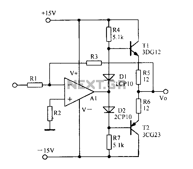
Current spreading bipolar output when the circuit diagram is as follows. The circuit described involves a current spreading bipolar output configuration. This type of circuit is typically used in applications requiring efficient current distribution across multiple output paths, often seen...