
555 Based Alarm Circuit
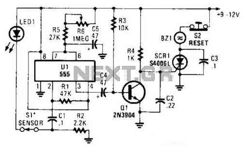
Transistor Q1 is heavily biased on by resistor R3, maintaining its collector at a level near ground. With Q1 in the on state, the gate of SCR1 is clamped to ground, preventing it from conducting. Once the delay circuit completes its timing cycle, pin 3 of U1 transitions to a low state, connecting the positive terminal of C4 to ground, which turns off Q1. As Q1 turns off, the voltage at the gate of SCR1 rises, activating the SCR and triggering the alarm. The duration of the delay can be adjusted from a few seconds (with resistor R6 set to its minimum resistance) to approximately one minute (with R6 adjusted to its maximum resistance).
The alarm circuit employs a 555 timer in a versatile dual role, enhancing its functionality and efficiency. The use of a normally-closed sensor switch ensures that the system remains in a dormant state until an unauthorized entry is detected, at which point the circuit is activated. The timing mechanism relies on the charging characteristics of capacitor C4, which, when charged, determines how long the system will remain in an active state before sounding the alarm.
The adjustment of resistor R6 provides flexibility in the timing cycle, allowing for customization based on the specific application requirements. This feature is particularly useful in installations where varying levels of security and response times are necessary. The integration of the transistor Q1 and SCR1 creates a robust mechanism for alarm activation, ensuring reliable performance under different conditions.
Overall, this alarm circuit design is an effective solution for monitoring and responding to unauthorized access, leveraging the capabilities of the 555 timer and associated components to provide a responsive and adjustable security system. The alarm circuit has a single 555 oscillator/timer (Ul) performing double duty; serving both in the alarm-trigger circuit arid the entry- delay circuit. In this application, the trigger input of IJ1 at pin 2 is held high via Rl. A normally-closed sensor switch, SI, supplies a positive voltage to the junction of R2 and CI, and lights LED1.
With both ends of CI tied high, there is no charge on CI. But when SI opens, CI (initially acting as a short) momentarily pulls pin 2 of Ul low, triggering the timed delay circle.At the beginning of the timing cycle, Ul produces a positive voltage at pin 3, which charges C4 to near the positive voltage at pin 3, which charges C4 to near the positive supply voltage. Transistor Q1 is heavily biased on by R3, keeping its collector at near ground level. With Q1 on, SCRl`s gate is clamped to ground, holding it off. When the delay circuit times out, pin 3 of Ul goes low and ties the positive end of C4 to ground. That turns Q1 off.When Q1 turns off, the voltage at the gate of SCR goes positive, turning on the SCR and sounding the alarm. The delay time is adjustable from just a few seconds (R6 set to its minimum resistance) to about one minute (R6 adjusted to its maximum resistance).
🔗 External reference
Related Circuits
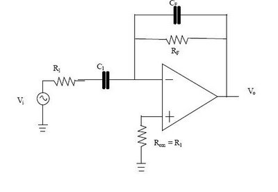
The differentiator circuit is an application circuit derived from mathematical principles influenced by capacitor behavior. The circuit, as illustrated in the accompanying image, is a simple differentiator configuration. To derive the differentiator formula, the following sequence is used: Ic...

This filter circuit, which utilizes the LM1458 or a similar operational amplifier, has a frequency response ranging from 300 Hz to 3.4 kHz, exhibiting a roll-off of 12 dB per octave outside the passband. Section A serves as the...
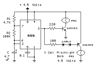
The 555 circuit below is a flashing bicycle light powered with three C or D cells (4.5 volts). The two flashlight lamps will alternately flash at an approximate 1.5 second cycle rate. Using a 4.7K resistor for R1 and...

The circuit depicted in Figure 3-201 includes two starting resistors, with one controlled by a time relay. A master switch (SA) is utilized to manage the motor's reversing operation. The circuit incorporates a reverse braking mechanism, which is automatically...

The following circuit illustrates a practical electronics astable circuit diagram based on the 555 Timer IC. This circuit produces a pulse frequency of approximately 2Hz with a very low mark-space ratio, making it suitable for various applications. The single...
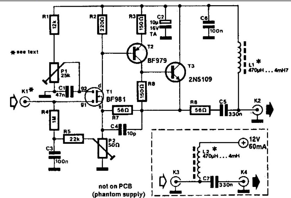
A whip antenna measuring between 30 to 50 cm is capable of receiving signals from 10 MHz to over 220 MHz. The circuit incorporates a BF981 dual-gate MOSFET (T1), which offers low noise characteristics, high input impedance, and enhanced performance. The...
Warning: include(partials/cookie-banner.php): Failed to open stream: Permission denied in /var/www/html/nextgr/view-circuit.php on line 713
Warning: include(): Failed opening 'partials/cookie-banner.php' for inclusion (include_path='.:/usr/share/php') in /var/www/html/nextgr/view-circuit.php on line 713