
555 DC/DC Converter
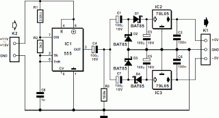
The circuit utilizes a 555 timer in astable mode, generating a continuous square-wave signal that serves as the foundation for voltage generation. The frequency of approximately 160 kHz is determined by the resistor values R1 and R2, which set the charge and discharge times of the timing capacitor within the 555 timer. The duty cycle, maintained near 50%, ensures that the output signal is balanced, providing equal time for high and low states.
Following the timer, the voltage-doubling rectifiers employ two sets of capacitors (C1, C3 for the positive side and C7, C5 for the negative side) and diodes (D2, D1 for the positive side and D4, D3 for the negative side). This configuration effectively doubles the amplitude of both the positive and negative halves of the square wave. The smoothing capacitors (C3 and C5) filter out the ripple from the rectified signals, yielding stable DC voltages that can be fed into standard linear voltage regulators.
The voltage regulators, typically 7805 for positive and 7905 for negative outputs, stabilize the voltages to +5 V and -5 V, respectively. These regulators are designed to handle input voltages within the specified range and provide a reliable output for powering low-power devices.
Overall, this circuit design is both efficient and practical for hobbyists and professionals alike, offering a simple solution for generating dual supply voltages in various electronic applications. Its compatibility with automotive voltage levels further enhances its usability in mobile applications.The circuit presented here may provide a solution in a number of cases, since it can be used to convert a single-ended supply voltage into a balanced set of supply voltages. That`s not so remarkable by itself, but the special feature of this circuit is that this is accomplished without using difficult to obtain, exotic ICs.
All of the components used in the circuit are ones that every electronics hobbyist is likely to have in a drawer somewhere. The heart of the circuit is formed by an old reliable` 555 timer, which is wired here as a free-running oscillator with a frequency of approximately 160 kHz. The oscillator is followed by two voltage-doubling rectifiers, consisting of C1, D1, D2, C3 and C7, D3, D4, C5.
They are followed in turn by two voltage regulators to stabilise the positive and negative voltages generated in this manner. The duty cycle of the 555 is set to approximately 50 percent using R1 and R2. The square-wave signal at the output of the timer IC has a DC offset, which is eliminated by C4 and R3.
The amplitude of the output signal from the 555 is approximately equal to the supply voltage less 1. 5 V, so with a 12-V input voltage, there will be a square-wave signal on pin 3 with an amplitude of approximately 10. 5 Vpp. With respect to ground (across R3), this is this +5 V / 5 V. Although this yields a symmetric voltage, its positive and negative amplitudes are somewhat too small and it is not stabilised.
In order to split the square-wave signal into sufficiently large positive and negative amplitudes, C1/D2 are added for the positive voltage, causing the positive half to be doubled in amplitude. For the negative half, the same effect is achieved using C7/D3. Following this, the two signals are smoothed by D1/C3 and D4/C5, respectively. Both voltages are now high enough to be input to normal 5-V voltage regulators, yielding symmetric +5V and 5V supply voltages at the output.
The input voltage does not have to be regulated, although it must lie between +11 V and +18 V. The maximum output current is ±50 mA with an input voltage of 12 V. This circuit is an excellent choice for generating auxiliary voltages, such as supply voltages for low-power opamps. Naturally, the fact that the converter can be powered from the in-vehicle voltage of a car is a rather attractive feature.
🔗 External reference
Related Circuits
A single hand clap will be picked up by the electric mic which is coupled through C1 into the op amp IC1. The output of IC1 triggers the 555 IC timer IC2 which is configured as a monostable multivibrator....
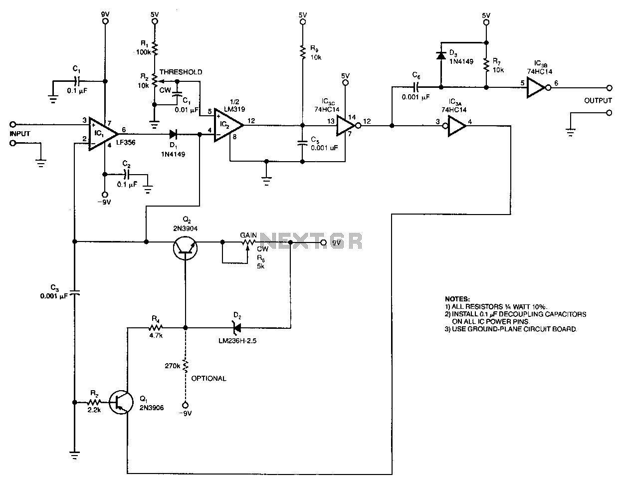
The output pulse width from the circuit is a linear function of the input pulse height. The circuit's input threshold can be set to discriminate against low-level pulses, while fixed components limit the maximum output pulse width. With a...
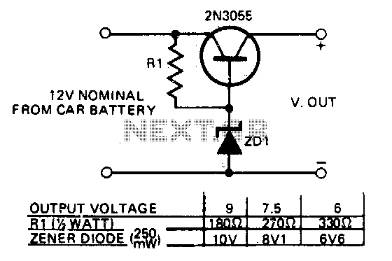
This circuit allows transistorized devices, such as radios, cassette players, and other electrical appliances, to operate from a car's electrical supply. The accompanying table provides resistor values and specifies diode types for different voltage levels. If multiple voltage levels...
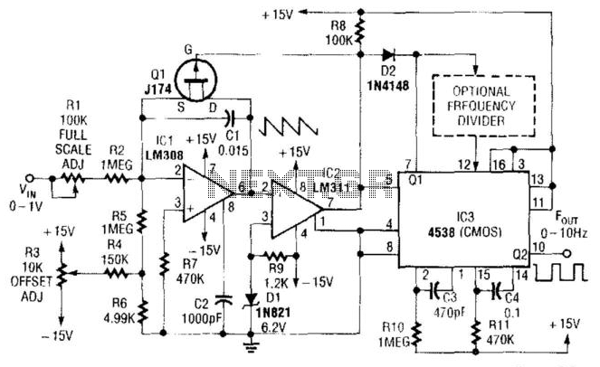
In this circuit, capacitor CI is charged to a fixed reference level and then discharged. The integrator IC1 charges CI until IC1 has a -6.2 V output, at which point comparator IC2 outputs a low signal. FET Q1 triggers...
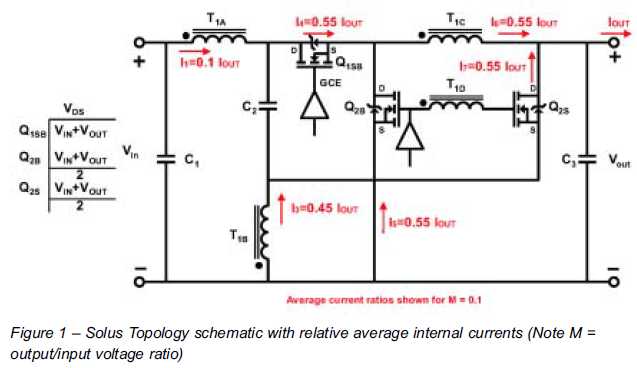
The ability to reduce power losses is crucial. This document describes a new ultra-high-performance topology that is expected to serve as the foundation for next-generation DC-DC power supplies in high-demand applications. The proposed ultra-high-performance topology aims to significantly enhance the...
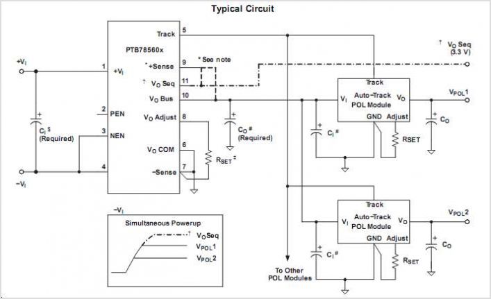
PTB78560BAS is a subpackage of PTB78560B. For a detailed description, please refer to PTB78560B. The datasheet for PTB78560BAS can be downloaded below. Provided by Texas Instruments. The PTB78560BAS is a specific variant within the PTB78560B family of components, designed for...