
555 Individual Pulse Width circuit
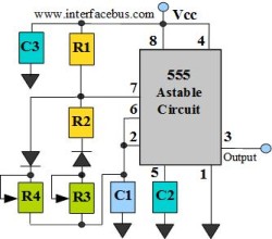
The astable multivibrator circuit is a versatile and widely used configuration in electronics for generating square wave signals. The operation of this circuit relies on the charging and discharging cycles of capacitor C1, which are influenced by the resistances of R1, R2, R3, and R4. The frequency of oscillation can be calculated using the formula:
\[ f = \frac{1.44}{(R1 + 2R2) \times C1} \]
This formula indicates that the frequency is inversely proportional to the total resistance in the timing circuit and directly proportional to the capacitance. The use of potentiometers allows for fine-tuning of the timing intervals, thus enabling customizable frequency output for various applications.
The diodes D1 and D2 play a crucial role in ensuring that the capacitor charges and discharges independently, which is essential for achieving a stable oscillation. When the capacitor is charged through R1 and R4, the voltage across C1 rises until it reaches the threshold level, causing the internal comparator to toggle the state of the output. Conversely, when discharging through R2 and R3, the capacitor voltage drops until it reaches the trigger level, at which point the cycle repeats.
The design considerations for this circuit also include the implementation of bypass capacitors (C2 and C3) for noise reduction and stability. These capacitors help filter out voltage spikes and provide a cleaner power supply to the 555 timer, which is critical for maintaining consistent operation.
Overall, the astable multivibrator circuit is not only a fundamental building block in timing applications but also serves as a basis for more complex circuits, including pulse-width modulation (PWM) and frequency modulation (FM) applications. Its adaptability and ease of implementation make it an essential component in the toolkit of electronics engineers and hobbyists alike.The Astable multivibrator circuit has no stable state. With no external signal applied, the internal transistors alternately switch from cutoff to saturation at a frequency determined by the RC time constants of the coupling circuits. So an Astable multivibrator is a square-wave oscillator with a oscillation frequency dependent on the value of the
resistor and capacitors used in the circuit. The basic Astable Multivibrator circuit is shown below; however the description of the circuit operation is provided on the 555 Astable Circuit page. This circuit arrangement allows for independent charge and discharge times by forcing the capacitor [C1] charging through R1 and R4 [potentiometer] and the discharging current through R2 and R3 [potentiometer].
The diodes [D1 and D2] control the flow of current through the individual resistors; however both resistor paths use the same capacitor [C1]. In this case potentiometers are added to the circuit to allow for adjustment of the resistance in the timing path.
However the potentiometers are not required and could be replaced with fixed resistors to control the charge and discharge times of the capacitor. Except for the addition of the potentiometers and the separate current paths created by the individual diodes, this circuit functions just like an Astable Multivibrator.
The circuit could be simplified further by replacing the two variable resistors [R3 & R4] with a single variable resistor. The two end of the resistor would be connected to each of the diodes and the center tap would connect to pin 2 of the 555.
The only issue with using one potentiometer is that the pulse widths are fixed together. So that as one period is increased [or decreased] the other period is decreased [or increased]. In addition a 50% Duty Cycle Oscillator is also possible using a different circuit arrangement. Although as the other page suggests a flip flop could be added to the output of the 555 to even out the duty cycle, which also happens to produce a binary divider. Clocking a 7473, with both the J & K inputs tied high, toggles the output each time the clock goes high [the clock to the flip flop is the output from the timer].
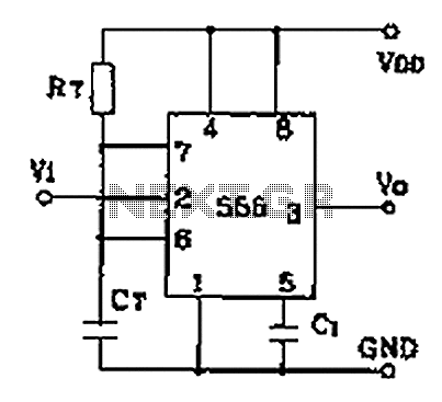
The 555 integrated circuit should have a 0. 1uF ceramic bypass capacitor [C3] between Vcc pin and ground; however the capacitor is not a requirement, just good design practice. In addition the Control Voltage [Pin 5] of the 555 is not used in this application so an optional 0. 01uF bypass capacitor [C2] is used between pin 5 and ground. This bypass capacitor is also optional, and pin 5 may be left open if required. Output: Pin 3 is the output of the circuit. The output will toggle or oscillate between ground and [near] Vcc. With Vcc set at 5 volts the output will switch to a minimum voltage of 2. 75 volts or a typical voltage of 3. 3 volts. Using a 15 volt Vcc as another example the 555 will typically reach 12. 5 volts [200mA source], 13. 3 volts [100mA source]. The rise and fall times of the output pulse will be about 100nS. Trigger: Pin 2 is connected to C1 which develops the voltage to the pin. The Trigger is also connected to the Threshold pin which also sees the same voltage. As the Trigger voltage [Vc] falls below 1/3 Vcc the internal comparator within the 555 will trigger. Threshold: Pin 6 is also connected to C1 which develops the voltage to the pin. The Threshold is also connected to the Trigger pin which also sees the same voltage. As the Threshold voltage [Vc] rises above 2/3 Vcc the internal comparator within the 555 will trigger.
Discharge: Pin 7 is connected between resistors R1 and R2. The capacitor C1 will charge through R1 and R4, but will only discharge through R2 and R3 into pin 7. This allows for a duty cycle that may be adjusted via the two potentiometers through the blocking diodes.
🔗 External reference
Related Circuits
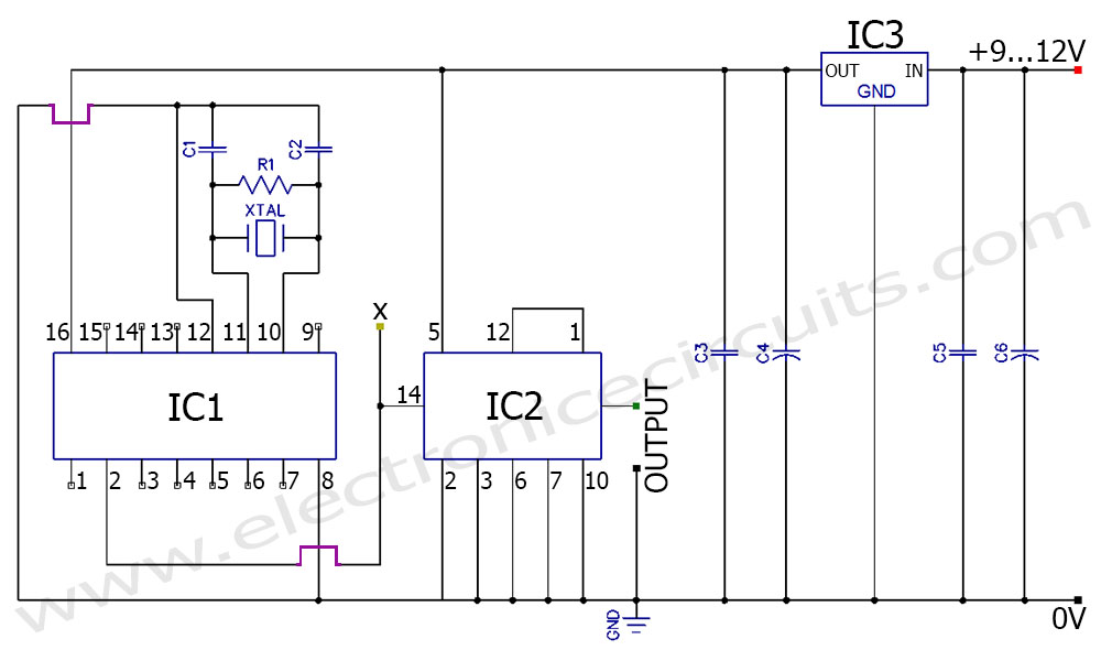
A frequency generator circuit capable of producing 50 Hz and 60 Hz outputs using a crystal oscillator. This oscillator can be utilized to generate precise frequency signals. This frequency generator circuit employs a crystal oscillator as its core component, which...
Two circuits for laser transmitters are described. The first circuit utilizes a simple laser pointer module, with 3 or 5mW devices functioning effectively. Higher power units are often imported from the USA or Hong Kong compared to UK approved...
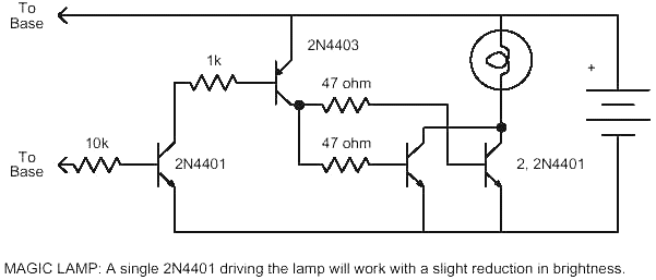
This magic lamp appears to be an ordinary frosted light bulb with a rather unusual characteristic. Whenever a finger touches the base threads and center contact, the lamp magically lights up without wires. It creates a compelling illusion if...
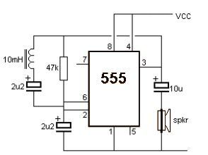
This metal detector electronic project schematic circuit is designed using a simple 555 timer integrated circuit. The schematic circuit requires few external electronic components. The metal detector circuit utilizes the 555 timer IC in an astable mode configuration, which generates...

This is a circuit diagram of a simple circuit in which the LED can be activated only by a gust of air. A condenser microphone (M1) is used to detect breath. When the S1 button is pressed, transistors Q2...
Common monostable circuit in two configurations: manual start type and start pulse type. It generates a single-shot pulse upon activation. A monostable circuit, also known as a one-shot multivibrator, is a fundamental electronic circuit that produces a single output pulse...