
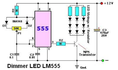
555 LED flasher
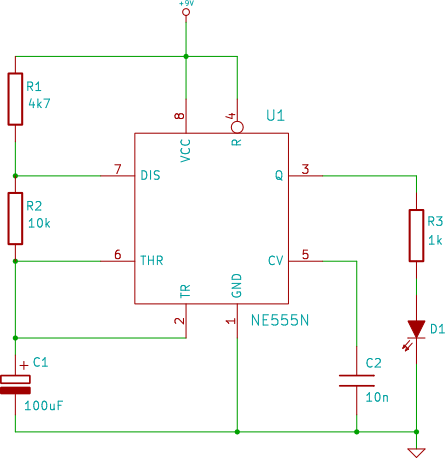
The circuit described utilizes a 555 timer IC configured in astable mode, which generates a square wave output that causes the connected LED to flash. The positive terminal of a 9V battery provides the necessary power supply, while the ground connection is essential for completing the circuit. The 555 timer's pins are connected as follows: pin 8 (VCC) connects to the positive rail, and pin 1 (GND) connects to the negative rail, establishing the power supply for the timer.
Capacitor C2, with a value of 10nF, is connected to pin 5 (control voltage) of the 555 timer, which helps stabilize the operation of the timer. The resistor R2 (10kΩ) connects pins 6 and 7, which are critical for setting the timing cycle of the output signal. The resistor R1 (4.7kΩ) connects pin 7 to the positive rail and helps determine the frequency of the output signal. The capacitor connected to pin 6, along with the resistors, sets the charge and discharge times, which in turn influences the flash rate of the LED.
Pin 3 of the IC serves as the output, where the 1kΩ resistor (R3) limits the current flowing through the LED, protecting it from excessive current that could cause damage. The LED’s anode connects to the output through R3, while the cathode connects to ground, completing the circuit.
This configuration allows the circuit to oscillate, resulting in the LED flashing on and off at a rate determined by the values of R1, R2, and C2. Proper verification against the schematic ensures that all components are connected correctly, enabling the circuit to function as intended.The connection point for the positive terminal of the 9V battery is displayed as a circle at the end of a line with the label "+9V". This is just another way of showing where to apply power to the circuit. The 0V or "GND" of the circuit is shown as an inverted triangle at the bottom of the circuit. This is where the negative lead of the battery mu st be connected. The schematic symbol for the 555 timer IC is not drawn to the layout of the physical 555 IC. I. e. it does not have pins 1 to 4 on one side and pins 5 to 8 on the other. Schematic symbols for IC`s are often laid out differently to the physical IC. This makes it easier to read the schematic diagram. Even though the pins are in different places in the schematic, they still have the correct pin numbers and names as the physical IC. Plug the 555 timer IC into the breadboard across the middle insulating channel. None of the IC`s pins will be shorted out because of the middle insulating channel. Using wire links, connect pin 8 of the IC to the top rail and pin 1 of the IC to the bottom rail. Get a wire link ready to connect between pins 6 and 2 of the IC. Connect one pin of the 10nF capacitor (C2) to pin 5 of the IC and the other pin of the capacitor to the bottom rail.
This is done using two wire links in the photo. Get wire links ready to connect pin 4 of the IC to the top rail. Connect the 10k resistor (R2) between pins 6 and 7 of the IC. Connect the 4k7 resistor (R1) between pin 7 of the IC and the top rail. Get the 100uF capacitor ready. Connect the 1k resistor (R3) to pin 3 of the IC. Connect the other pin of the resistor into a free connecting strip of the breadboard. Connect the anode of the LED to R3 and the cathode of the LED to the bottom rail. Check the circuit that you have built against the schematic diagram. Go around the IC and check that each pin is connected to what the schematic says it must be connected to. If you are sure that your circuit is correct, connect the positive lead of the 9V battery to the top rail and the negative lead to the bottom rail and watch the LED flash on and off.
🔗 External reference
Related Circuits
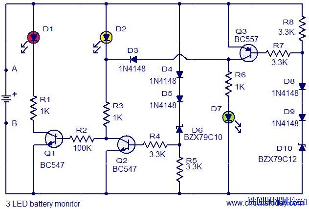
This is the circuit diagram of a 3 LED bar graph type battery monitor circuit that is ideal for monitoring the voltage level of an automobile battery. When battery voltage is 11.5V or less, transistor Q1 will be on...
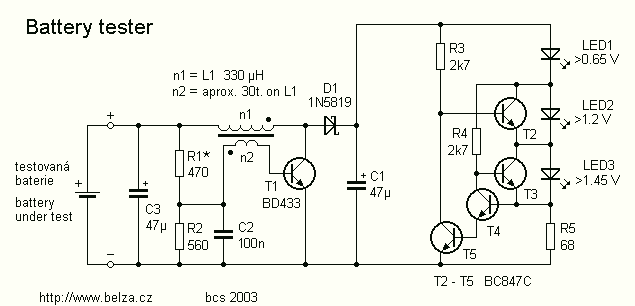
The device serves to quickly establish the status of an indicative power cells. I built it for his children, so they can determine the degree of self-discharge batteries in a variety of toys. WAS tester designed to test the...
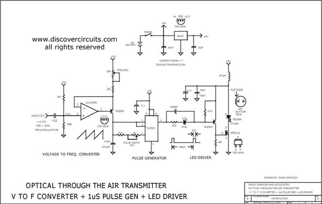
This circuit receives the signal from the amplifier and emits powerful 1μs infrared light pulses from a low-cost LED, which are frequency modulated by the audio information. The 10kHz center frequency of the pulse stream is sufficiently low, allowing...
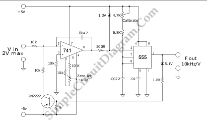
A voltage-to-frequency converter (VFC) circuit is illustrated in the schematic diagram below. The circuit utilizes a 555 integrated circuit (IC) as the central component of its operation. The voltage-to-frequency converter (VFC) is a crucial electronic circuit that converts an input...
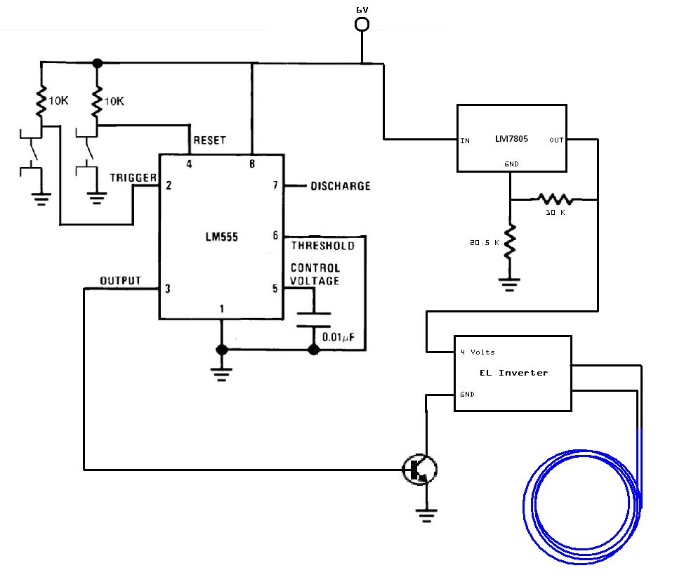
The circuit utilized for this project is quite simple. Some may criticize the omission of decoupling capacitors for the LM7805 voltage regulator. The circuit in question employs the LM7805 voltage regulator, which is designed to provide a stable output voltage...
The LM555 timer IC can be utilized in various electronic projects, including the creation of an analog timer. According to the datasheet, the LM555 is versatile and can be adjusted to set timers based on specific requirements. The schematic...