
555 meter circuit diagram of the analog information Qigong
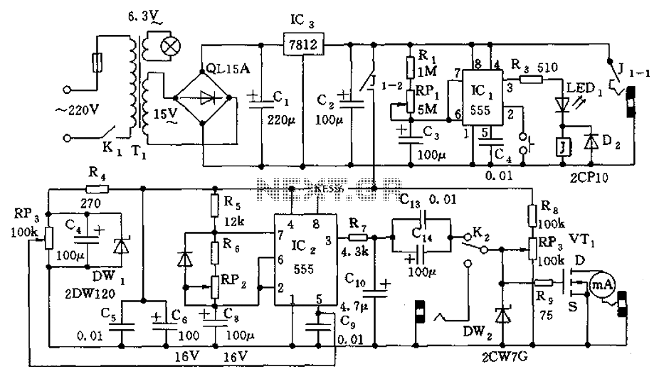
The described apparatus is a sophisticated electronic system that integrates several key components to achieve its operational goals. The buck rectifier power supply is essential for converting higher voltage levels down to a stable +12V, which is necessary for powering the subsequent circuitry. The timing circuit is crucial for establishing precise intervals for operation, with R1, RP1, and C3 forming a timing network that determines the duration of the timing cycle. The timing calculation, td = 1.1(R1 + RP1)C3, indicates that the timing duration is influenced by the resistance values of R1 and RP1, as well as the capacitance of C3.
The control mechanism involving J pull and the connections at J1-1 and J1-2 suggests that the timing circuit may interface with other parts of the system, enabling or disabling functions based on the timing state. The multivibrator, managed by IC2 and supported by resistors R5, R6, RP2, and capacitor C8, generates oscillations at a frequency defined by the equation f = 1.44/(R5 + 2R6 + RP2)C8. This configuration allows for flexibility in frequency modulation, which can be fine-tuned through the addition of a control voltage at the 5-pin connector, specifically by adjusting RP3.
The use of a V-MOS field-effect power transistor (VT1) enhances the power handling capabilities of the circuit, enabling efficient switching and amplification of signals. The output head's design, incorporating a 0.85μm GaAs semiconductor laser, indicates a focus on applications requiring infrared radiation, which is facilitated by the PTC special ceramic material. This setup, combined with the strong magnetic fields produced by SmCo magnets, suggests that the apparatus is designed for applications in fields such as telecommunications, laser-based systems, or other advanced electronic applications where precise timing and control are critical. As shown, the information apparatus comprises buck rectifier power supply (Vdd + 12V), the timing circuit, multivibrator, the output of the first amplifier and function. IC1 an d R1, RP1, C3 composition start timing, timing td 1.1 (R1 + RP1) C3. In the timing, J pull, control J1-1, J1-2 contacts connected. IC2 and R5, R6, RP2, C8 and other components controlled multivibrator, f 1.44/(R5 + 2R6 + RP2) C8, but the frequency can be changed by adding 5 feet in control voltage, namely by adjusting to RP3 achieve. VT1 using V-MOS field-effect power transistor. Function output head adopts 0.85um GaAs semiconductor laser and infrared radiation PTC special ceramic material, and a strong magnetic field SmCo magnets.
Related Circuits

This light sensor circuit, utilizing a photosensor, serves as a bridge between light and electronics. It is constructed using an operational amplifier and the PIC16C63 microcontroller to control the sensor. While the circuit is not intended for precision applications,...
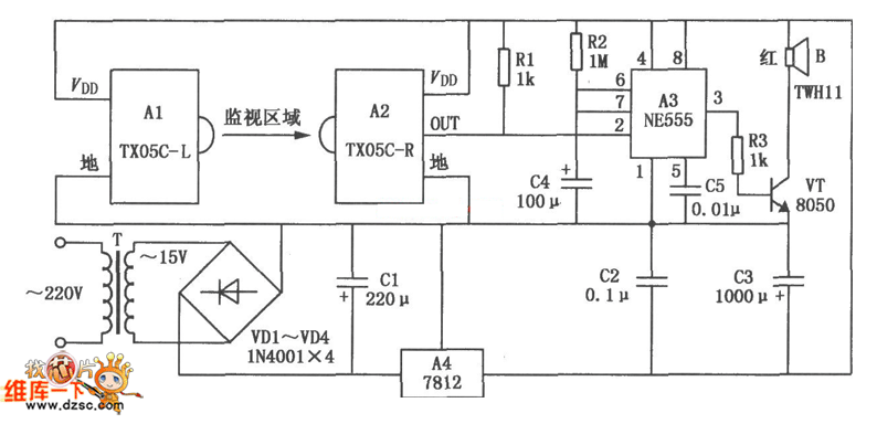
The TX05C-R infrared surveillance alarm circuit is designed for monitoring walls, windows, doors, and various restricted areas. When an intrusion occurs, the alarm activates to enhance security. The circuit comprises a transmitter module, a receiver module, a time-base circuit,...
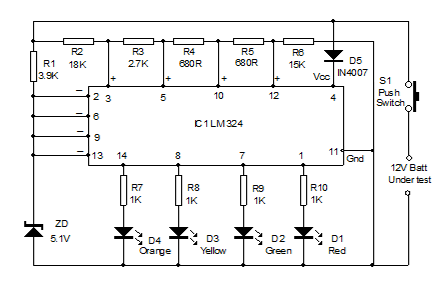
Battery Volt Meter Circuit Diagram. This circuit is designed to monitor the voltage level in Lead Acid or Tubular batteries. It provides four LED indicators to represent the voltage levels ranging from 9 volts to 14 volts. The battery voltmeter...
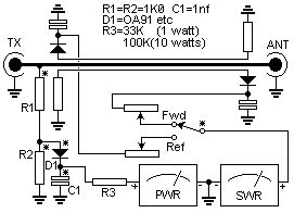
Many SWR (Standing Wave Ratio) and power meters used by amateur radio operators provide reasonably accurate continuous average power readings with a CW (Continuous Wave) key-down signal. However, these meters may not reliably measure Peak Envelope Power (PEP) or...
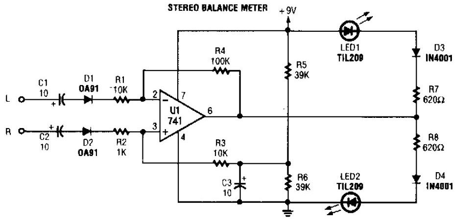
The simplest stereo balance meter circuit schematic available on the internet. When the left and right signals are equal, no output is present from U1 and pin. This stereo balance meter circuit is designed to visually indicate the balance between...
This voltmeter ammeter is designed to measure output voltage ranging from 0-70V to 0-500V with a resolution of 100mV and can measure current from 0-10A or more with a resolution of 10mA. It is an ideal addition to any...