
555 monostable trigger timing circuit
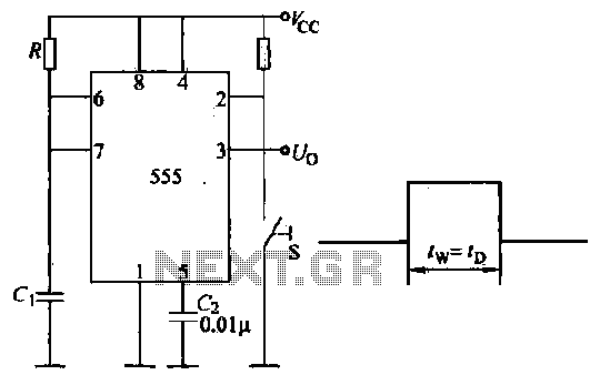
The circuit schematic in Figure 3-3 illustrates a monostable configuration of the 555 timer, which is a popular integrated circuit used for timing applications. In this setup, the 555 timer is triggered by a normally open push button switch, which initiates the timing cycle. When the button is pressed, the circuit transitions from a low output state to a high output state, resulting in a voltage increase at the output pin. This transition is facilitated by the internal flip-flop of the 555 timer, which changes state in response to the activation of the push button.
The timing behavior of the circuit is governed by the resistor (R) and capacitor (C) connected to the 555 timer. The time period for which the output remains high, known as the pulse width, is calculated using the formula TW = 1.1RC. This means that the time duration is directly proportional to both the resistance and capacitance values selected. A larger resistor or capacitor will result in a longer output high time, while smaller values will shorten this duration.
When the button is released, the internal discharge switch (Ij1) activates, discharging the capacitor and returning the output to a low state. This allows the circuit to reset and be ready for the next activation. The monostable operation of the 555 timer makes it suitable for applications where a single output pulse is needed in response to an input trigger.
In terms of component selection, the circuit does not impose any stringent requirements, allowing for flexibility in choosing the resistor and capacitor values to achieve the desired timing characteristics. The schematic serves as a fundamental example of how a 555 timer can be employed in a practical circuit for generating timed pulses, showcasing its versatility in electronic design.Introduction to circuit schematic of the circuit shown in Figure 3-3. Here the 555 connected as a one-shot form, usually in a normally open push button switch S-shaped state, pin output low 555. At this point the internal discharge switch Ij1 together, the voltage across capacitor C is zero. When you press the button switch S, the flip-flop flip, 555 feet from low to high, electrical path into the temporary steady state. After Zhe state time, the output end electrostatic level goes low. Transient time - as is the timing TW '- 1. 1RC. This circuit each press switch S, the circuit enters a given working condition once, so this circuit is brother to manually control the development work of the occasion.
(2) Component Component selection parameters as shown in Figure 3-3 shows, wife no special requirements. (3) 555 monostable trigger timing circuit shown in Figure 3-3.
Related Circuits
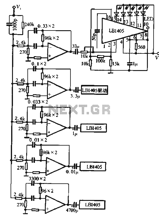
The circuit utilizes the LM324 as a band-pass filter and the LB1405 as a driver for a five-band spectrum display. The selected frequency harmonics are centered at 100 Hz, 330 Hz, 1 kHz, 3.3 kHz, and 10 kHz. The...
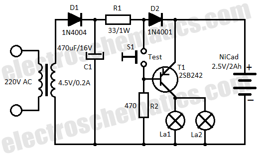
This low-cost automatic emergency lighting circuit activates a lamp during power failures. It is powered by a NiCad battery that is charged by the mains. The automatic emergency lighting circuit is designed to provide illumination during unexpected power outages. The...
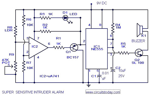
The circuit diagram illustrates an ultra-sensitive intruder alarm. The mere shadow of an intruder passing within a few meters of the circuit is sufficient to activate the alarm. In this setup, the IC2 uA741 is configured as a sensitive...
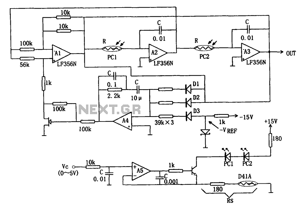
The wideband sinusoidal voltage-controlled oscillator circuit is designed such that the oscillation frequency is determined by an integrating resistor R and a capacitor C. The voltage-controlled oscillator is constituted by the applied control voltage Vc and a control resistor...
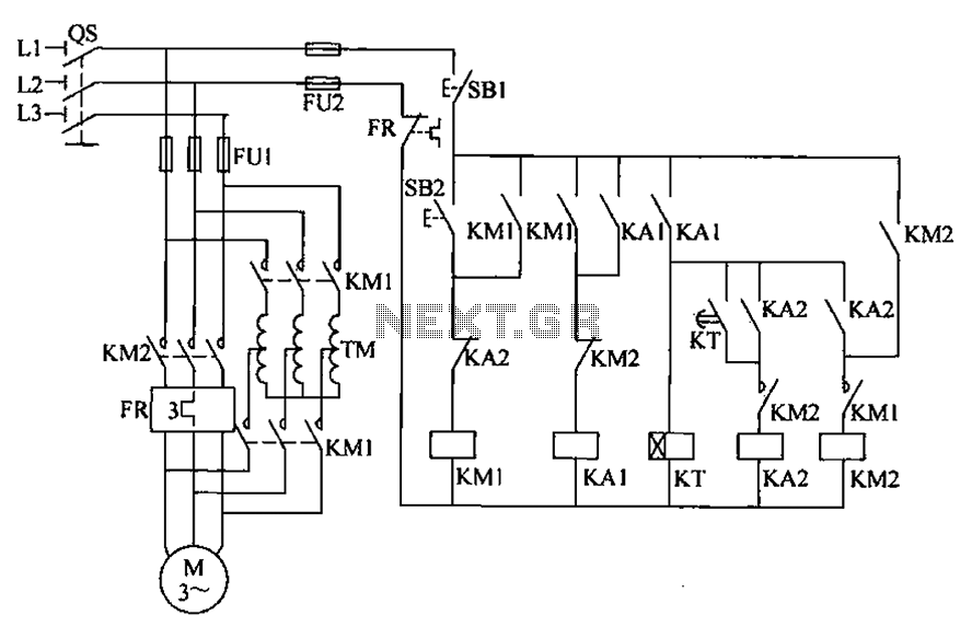
To initiate the system, turn off the power switch, then press the start button SB2. The KM1 contactor is energized, engaging self-locking, and closing the main contacts. The autotransformer TM is connected between the power source and the motor,...
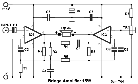
This is a compact collection of amplifiers configured in a bridge connection. The output power is low, making them suitable for general applications. They can be utilized with small active loudspeakers, car stereos, and similar devices. The only limitation...
Warning: include(partials/cookie-banner.php): Failed to open stream: Permission denied in /var/www/html/nextgr/view-circuit.php on line 713
Warning: include(): Failed opening 'partials/cookie-banner.php' for inclusion (include_path='.:/usr/share/php') in /var/www/html/nextgr/view-circuit.php on line 713