
555 Tester circuit
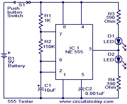
The NE555 timer in astable mode operates continuously, producing a square wave output without requiring any external triggering. The configuration involves connecting the discharge pin (pin 7) to a resistor network composed of R1 and R2, which sets the timing intervals for the charging and discharging phases of the timing capacitor, C1. The values of R1 and R2, along with the capacitance of C1, can be calculated using the formula for the frequency of oscillation:
\[ f = \frac{1.44}{(R1 + 2R2) \cdot C1} \]
This frequency determines how fast the LEDs will flash. The duty cycle, which indicates the proportion of time the output is high compared to the total period, can also be adjusted by varying R1 and R2.
The push button switch S1 serves as a manual trigger for the circuit, initiating the oscillation process. When pressed, it allows C1 to charge, and the subsequent voltage levels at the threshold and trigger pins (pins 6 and 2, respectively) dictate the operation of the flip-flop inside the NE555. The LED indicators D1 and D2 provide a visual representation of the output state, allowing for easy observation of the circuit's operation.
The design ensures that the circuit will function correctly as long as the NE555 timer is operational, with the timing components (R1, R2, C1) selected to achieve the desired flashing rate and duration. Proper selection of these components is crucial for achieving the intended performance of the circuit.Here the NE555 is wired as an astable multivibrator. When the push button switch S1 is pressed the LEDs D1 & D2 will flash alternatively. That is when output is high D2 will glow & when output is low D3 will glow. The rate of flashing will depend on components R1, R2 & C1. When push button S1 is pressed, C1 will start charging through R1&R2. When the voltage across C1 rises above 2 of 3 is the supply voltage the internal Flip Flop toggles. The pin 7 becomes low & C1 starts discharging. When the voltage across C1 goes below 1of 3 of supply voltage the internal Flip Flop resets & pin7 goes high. The C1 again starts charging. All this will take place if the IC is healthy. 🔗 External reference
Related Circuits
The rice cooker notification circuit operates as follows: When the rice cooker is in operation, both terminals A and B have a voltage of 0, meaning the entire circuit remains inactive. In the event that the rice cooker runs...
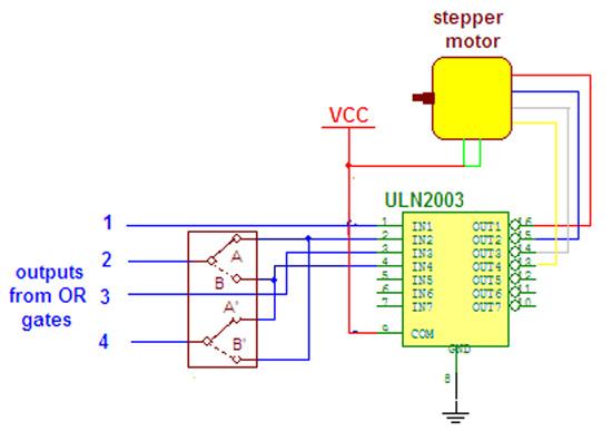
Wireless stepper motor speed control project using a laser and IC555. This project provides insights into the fundamentals and circuit construction for controlling the speed of a wireless stepper motor utilizing a laser and the IC 555 timer. The project...
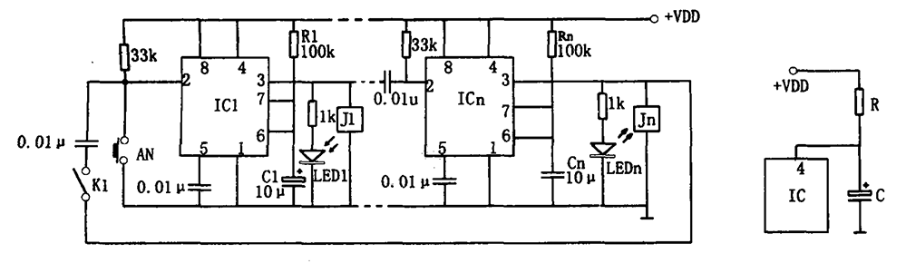
All integrated circuits (ICs) are equipped with a 0.1 µF monolithic ceramic capacitor connected across their terminals. Additionally, each board features two capacitors: a 10 µF tantalum capacitor and a 100 µF electrolytic capacitor. The START BUTTON serves as...
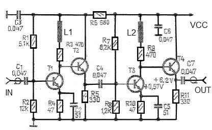
A simple and effective antenna amplifier can be built using the provided circuit diagram. This amplifier is designed for the frequency range of 35 kHz to 150 MHz. It utilizes transistors, offering a low non-linearity of 3 dB and...
The multi-channel temperature measurement circuit is illustrated in the figure. The core of the test circuit comprises a 555 one-shot delay circuit. When the button is pressed, the output pin of the 555 timer (IC1) goes high due to...
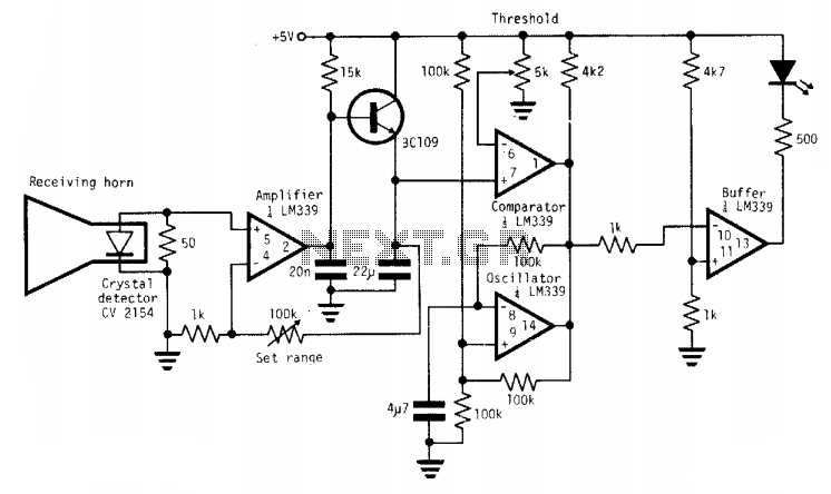
A simple X-band radar detector can indicate changes in RF radiation strength at levels as low as 2 mW/cm². When radiation strikes the detector diode, it generates a voltage at the input of an amplifier. The gain of this...