
555 timer astable multivibrator
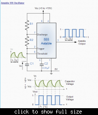
The astable multivibrator circuit is a type of oscillator that continuously switches between its high and low states, generating a square wave output. This circuit typically consists of two resistors (R1 and R2), a capacitor (C), and a bipolar junction transistor (BJT) or operational amplifier (op-amp) configured to operate in a feedback loop.
The duty cycle, defined as the fraction of one period in which a signal or system is active, is crucial for determining the output waveform characteristics. In this context, the formula d = (R1 + R2) / (R1 + 2 * R2) calculates the duty cycle based on the resistors' values. The components' values influence the frequency and duty cycle of the output waveform, which can be adjusted by changing R1, R2, or C.
In a typical astable multivibrator setup, the output frequency (f) can be derived from the formula f = 1.44 / ((R1 + 2 * R2) * C). This relationship indicates that both the resistor and capacitor values directly affect the frequency of oscillation. The output waveform will alternate between high and low states, with the duration of each state determined by the duty cycle.
The astable multivibrator can be implemented using various configurations, such as using a 555 timer IC or discrete components. The choice of components and their values will dictate the performance characteristics of the circuit, including the stability of the output frequency and the precision of the duty cycle.
In summary, understanding the duty cycle and its calculation is essential for designing astable multivibrator circuits that meet specific timing requirements. The ability to manipulate R1, R2, and C allows for a wide range of applications, from simple LED blinkers to more complex timing circuits in digital electronics.In the following astable multivibrator circuit, in some books, it is mentioned that the duty cycle id d=( R1+R2)/(R1+2*R2) in some other books, it is.. 🔗 External reference
Related Circuits
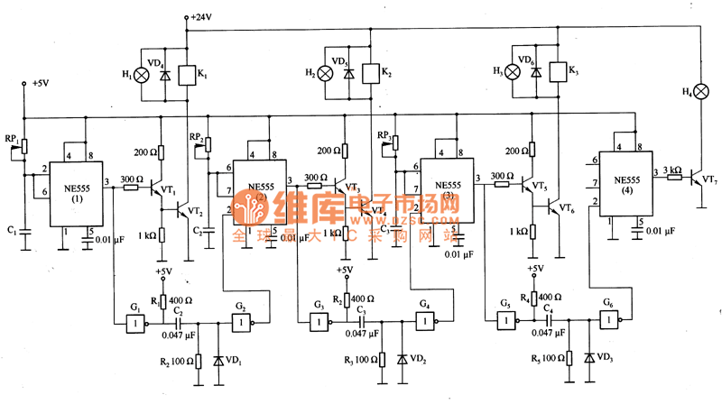
This is a sequence timer diagram composed of an NE555 timer. The timer can be set to any duration when the power is connected, allowing it to control an external system. In the circuit, K1-K3 are relays used to...
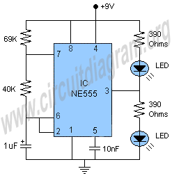
A project of a 555 tester circuit, the circuit will start blinking LEDs when power is applied, which will indicate that the IC is working correctly. The 555 tester circuit is designed to verify the operational status of the 555...
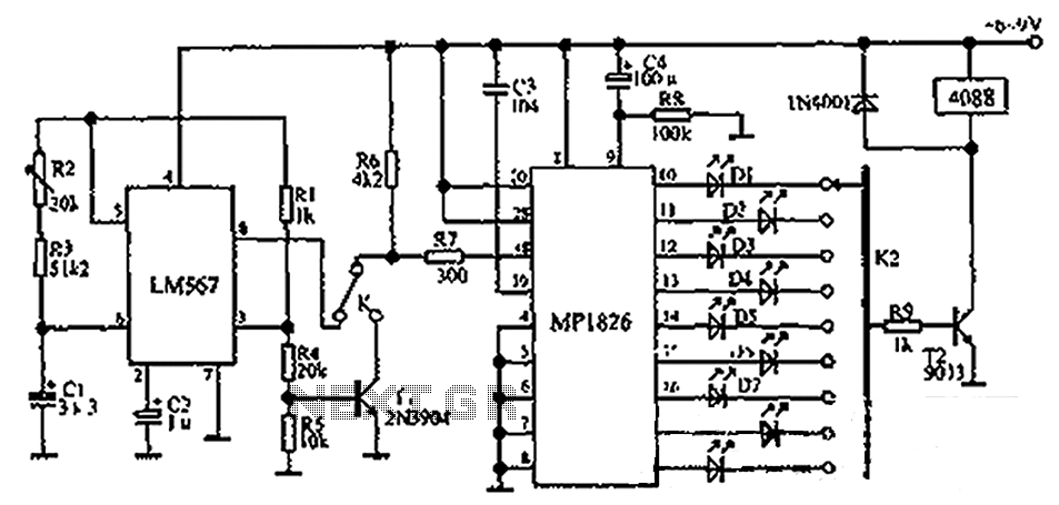
The circuit illustrated in the figure incorporates the MP1826 as a multi-stage divider. The LM567 serves as the frequency demodulation component, functioning as a dual-band oscillator that generates the desired low-frequency pulse from the MP1826. The oscillation center frequency...
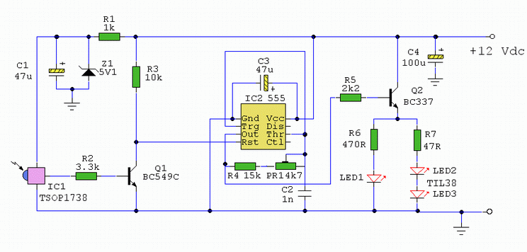
The following circuit illustrates the use of a 555 integrated circuit (IC) for an infrared (IR) remote control extender circuit. Features include support for 850 nm and 950 nm signal wavelengths, along with the capability to generate control pulses. The...
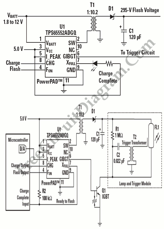
The size of the photoflash charger circuit is significantly simplified and reduced by the Texas Instrument (TI) TPS65552A. This device serves as a photoflash capacitor charger. The TPS65552A is a highly integrated photoflash capacitor charger designed to efficiently charge capacitors...
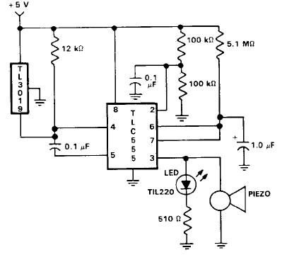
This door open alarm electronic project is designed using a linear hall effect device and a 555 timer circuit. The project utilizes the TL3103 linear hall effect device for detecting the angle of rotation. The TL3103 is positioned within...
Warning: include(partials/cookie-banner.php): Failed to open stream: Permission denied in /var/www/html/nextgr/view-circuit.php on line 713
Warning: include(): Failed opening 'partials/cookie-banner.php' for inclusion (include_path='.:/usr/share/php') in /var/www/html/nextgr/view-circuit.php on line 713