
lm567-mp1826 precision timer circuit diagram

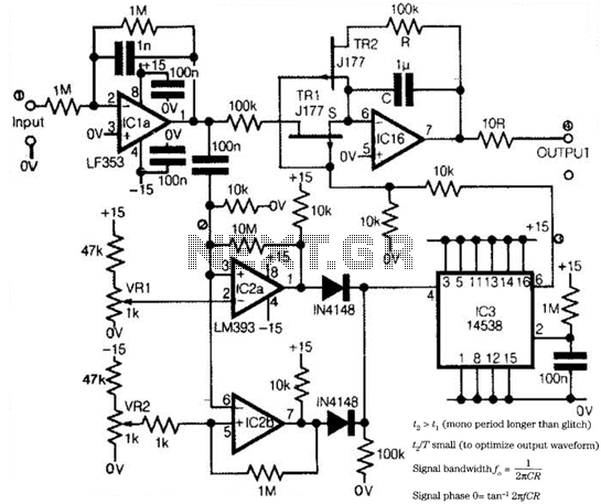
The MP1826 operates as a multi-stage frequency divider, which is particularly effective for generating low-frequency signals from a higher frequency input. The LM567, a versatile phase-locked loop (PLL) integrated circuit, is utilized for demodulating frequency signals. It is capable of processing dual-band frequencies, making it suitable for applications that require precise frequency generation and demodulation.
In this configuration, the oscillator's frequency (f0) is primarily determined by the values of C1, R2, and R3. The relationship between these components and the output frequency can be expressed through the formula f0 = 1/(2πRC), where R is the equivalent resistance and C is the capacitance in the timing circuit. The ability to adjust the time constant by changing these component values allows for a broad frequency range, thus enhancing the circuit's versatility.
The operation sequence begins with the activation of the circuit, during which the MP1826 resets, indicated by the flashing of D1. This initial state is crucial for ensuring that the circuit starts from a known condition. Following the reset, the low-frequency pulse generated at the output of the MP1826 is fed into the circuit, triggering a series of events that manipulate the state of various output pins. The timing intervals T and T2 are critical for controlling the transitions of pins 10 and 11, which in turn influence the subsequent states of pins 12 through 17.
The grounding of pin 8 serves as a control mechanism that initiates the timing sequence, culminating in the high state of pin 24 after a predetermined duration. This feature allows the circuit to function effectively as a timer, providing a timing gear of 18 without necessitating modifications to the component values. Such functionality is beneficial in applications where precise timing and frequency control are essential, such as in communication systems, signal processing, and automated control systems. Overall, the circuit's design emphasizes flexibility and precision in frequency generation and timing applications. As shown in FIG, MP1826 in the circuit as a multi-stage divider. LM567 is the frequency demodulation circuit, the circuit as a dual-band oscillator which generates the desired low-frequency pulse MP1826. Whose oscillation center frequency f0 determined by C1, R2, R3. f0 by a 3-pin output LM567, the 8-pin output 2f0. Changing circuit time constant, f0 may vary between 0.01Hz ~ 500kHz. This circuit f0 is 4Hz. When the circuit is turned on to work first MP1826 reset, then you can see D1 flashes a few times off. Low-frequency pulse input MP1826, after time T, 10 pin goes high, 11 feet and then after time T2 goes high, pin 10 goes low; the process of 12 to 17 feet and so on.
When the 8-foot ground, after 105XT2 time, 24 pin goes high. Circuit timer expires. Circuit without changing element parameters can have a timing gear 18.
Related Circuits
This circuit is designed to drive a total of 42 LEDs, assuming a forward voltage of approximately 2.2V per LED and a forward current of around 21mA for adequate brightness. If the specifications of the LEDs differ significantly, modifications...
Low-frequency signals produced by transducers, measurement equipment, or data loggers often resemble the first waveform in the figure. The circuit operates as a tracking sample-and-hold, where transients are replaced in the output by the stored value of the current...
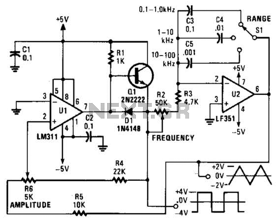
This is a simple triangle-wave generator utilizing two integrated circuit (IC) devices and a transistor. The triangle wave serves as feedback to the square-wave generator. It allows range switching across three intervals from 100 Hz to 100 kHz. Additional...
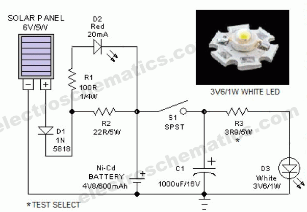
The 5W/6V solar panel can achieve a maximum current of approximately 500 to 800mA, peaking at 800mA during noon. Limiting the current to 150mA appears inefficient. A 1W panel can supply around 160mA during peak performance for up to...
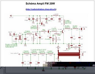
The following circuit illustrates an RF amplifier designed for FM frequencies ranging from 88 to 108 MHz with a broadband configuration. This circuit utilizes the BLV10 transistor. The RF amplifier circuit operates within the FM broadcast band, which is crucial...
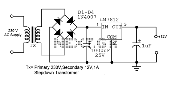
This is a straightforward 12V power supply circuit diagram. It features a fixed voltage output and is based on the LM7812 voltage regulator integrated circuit. The 12V power supply circuit utilizing the LM7812 voltage regulator is designed to provide a...