
555 timer ic operation
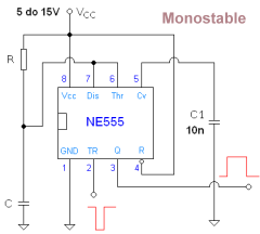
The 555 Timer is a versatile and widely used integrated circuit that can function in various configurations, including monostable, astable, and bistable modes. In the monostable mode, as described, the circuit produces a single output pulse in response to a trigger signal. The duration of this output pulse is determined by the values of the resistor (R1) and the capacitor (C1) connected to the timer. The relationship between these components is characterized by the formula:
\[ T = 1.1 \times R1 \times C1 \]
where \( T \) is the time period of the output pulse. The timer's operation is influenced by the charging and discharging characteristics of the capacitor, which are governed by the RC time constant.
In practical applications, the 555 Timer's output can drive various loads, such as LEDs, relays, and other electronic components, making it suitable for timing applications, sound generation, and pulse-width modulation. The ability to operate over a wide voltage range (4.5V to 16V) enables the 555 Timer to be integrated into diverse electronic systems, enhancing its utility in both hobbyist and professional designs.
When designing circuits with the 555 Timer, it is crucial to consider the impact of external components on performance. For instance, the choice of R1 and C1 will directly affect the timing accuracy and stability of the output pulse. Additionally, careful attention should be paid to the bypass capacitor connected to Vcc, ensuring that power supply fluctuations do not adversely affect the timer's operation.
In summary, the 555 Timer is a fundamental component in electronics, providing a reliable means of generating precise timing signals and facilitating various circuit functions. Its ease of use, combined with extensive documentation and support, makes it a staple in both educational and professional electronic design.The 555 Timer is an integrated circuit used as a timer, a pulse generator, tone generator and many other circuit functions, all from one universal IC function. Each pin function is described and design recommendation are given when required. A Monostable Multivibrator setup is used as an example to describe the operation of the 555. The basic bloc k diagram for the 555 timer is shown in the graphic below and referenced by the text. Note the term Vcc is used because the 555 will operate with any Vcc [pin 8] between 4. 5 volts and 16 volts. The actual voltage used by the 555 does not effect the timing circuit because both the charging rate of the capacitor and the threshold of the capacitor use the same voltage. As with any integrated circuit always Bypass the Vcc pin to ground with a 0. 1uF ceramic capacitor [not shown in the circuit below]. Pin 8 is Vcc and Pin 1 is ground; however the capacitor should be connector to Vcc and taken to the closest possible ground, which may not necessarily be pin 1 of the IC.
A by-pass capacitor is also called a Decoupling Capacitor. The 555 IC may be operated with any voltage between 4. 5 volts and 16 volts [see data sheet info below]. Select the Vcc voltage based on the circuit being driven by the 555 timer. The [trigger] input to the 555 is only being used as a reference switch so the actual voltage used is not important as long as the input transitions past the reference point [more below]. The 555 uses two comparators to control the operation of the timer. The lower comparator is set to trigger at 1/3 Vcc while the upper comparator is set to trigger at 2/3 Vcc.
Three internal 5k resistors placed in series between Vcc and ground are used to provide voltage references. The 1/3 Vcc voltage is generated between the bottom and middle 5k resistors and the 2/3 Vcc voltage is generated between the middle and upper 5k resistors.
The Trigger input [TRIG] is applied to the first comparator which is referenced to the 1/3 Vcc. So as long as the trigger voltage remains above 1/3 Vcc the 555 will not trigger [operate]. The second comparator is referenced to 2/3 Vcc and is used to discharge the timing capacitor C1 once the voltage across the capacitor reaches 2/3 Vcc. In addition to the external capacitor an external resistor is also required to complete the timing circuit.
The resistor [R1] and the capacitor [C1] form an RC circuit which define the length of time it takes the capacitor to charge [defined by this RC Curve ]. The discharge of the capacitor is completed through an internal transistor which is controlled by the two comparators.
Before the Trigger pulse occurs the internal transistor is `ON` [conducting] so the capacitor is effectively shorted to ground and is not allowed to charge. Once the trigger is applied and falls below 1/3 Vcc the comparator trips and turns the transistor off.
When the transistor shuts off the capacitor is allowed to charge toward Vcc. In effect the above text describes the operation of a monostable circuit. As the output will toggle once the negative trigger pulse is applied and will remain high until the capacitor reaches 2/3 Vcc and is again shorted out [discharged] by the internal transistor. The output will switch back to its resting state [low]. The top waveform is the input trigger pulse applied to pin 2. The center waveform represents the charging voltage on capacitor C1. While the bottom voltage waveform shows the resultant output on pin 2. Internally the 555 uses a buffer to drive the output pin capable of about 200mA of sink current [depending on the load].
However the output pulse could have a rise or fall time in the range of 100nS. Back in mid 1970s` a transition time of 100nS would be normal, these days 100nS is extremely slow and could cause problems if used as an input to high speed logic devices. Pin 3 is the output of the circuit. The output will toggle between ground and Vcc each time a 🔗 External reference
Related Circuits
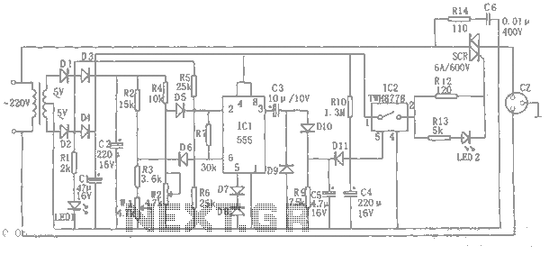
A collection of drawings showcasing various applications of the 555 timer IC. These include schematic diagrams sourced from online resources and literature, intended for personal reference. The original web pages from which these schematics were derived have not been...
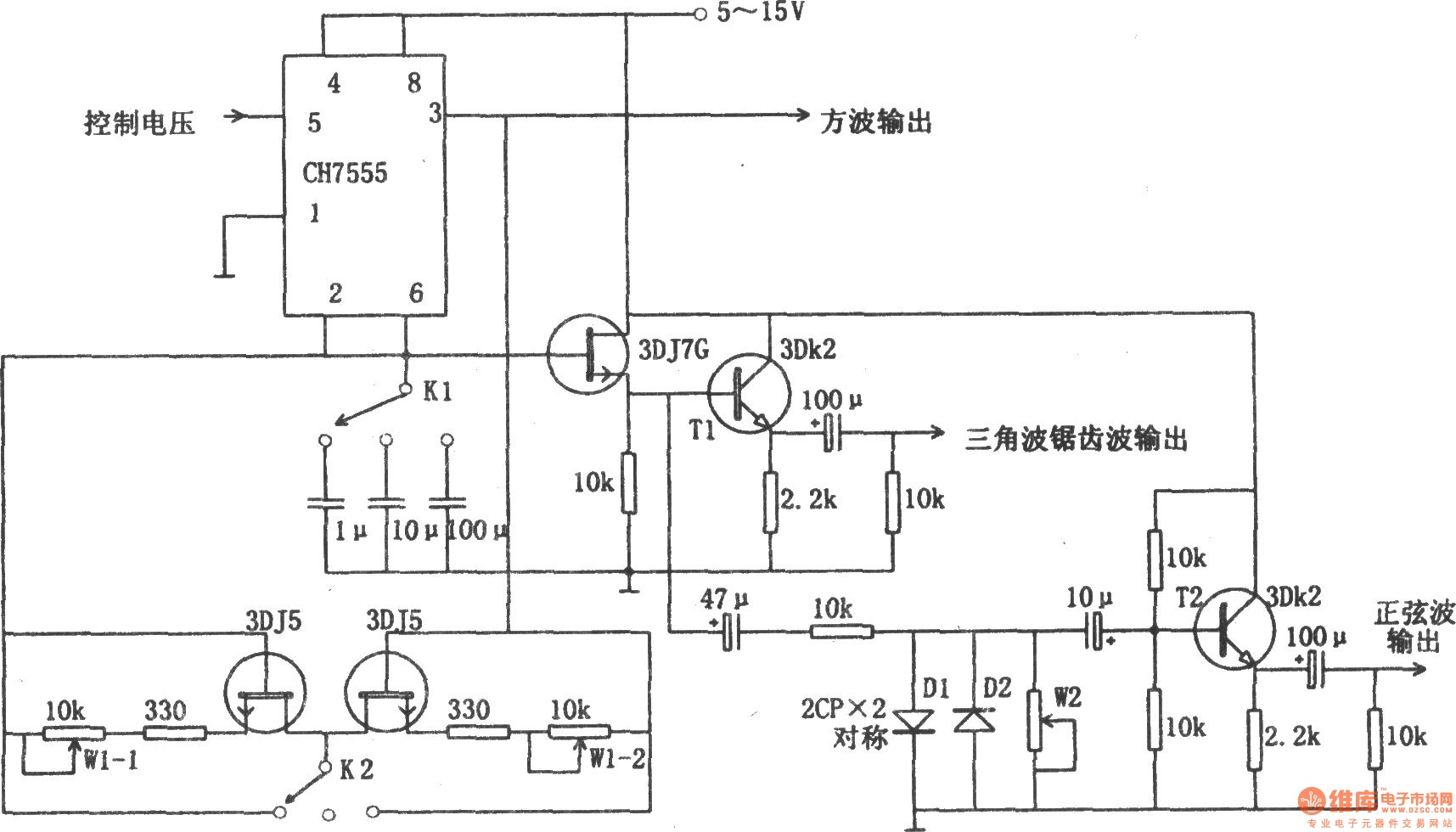
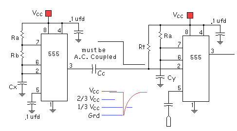
The chart illustrates a function generator circuit utilizing a 555 timer. This circuit includes a CH7555 timer along with several transistors and RC components. It is capable of generating triangle waves, square waves, sine waves, sawtooth waves, and square...
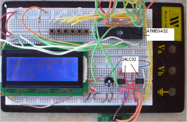
This circuit is a church bell controller. Basic component is an ATmega32 microcontroller. At the circuit 2 24LC32 EEPROM memories is being used, the 1st for internal standard melodies and the 2nd one is for user's compositions. This feature...
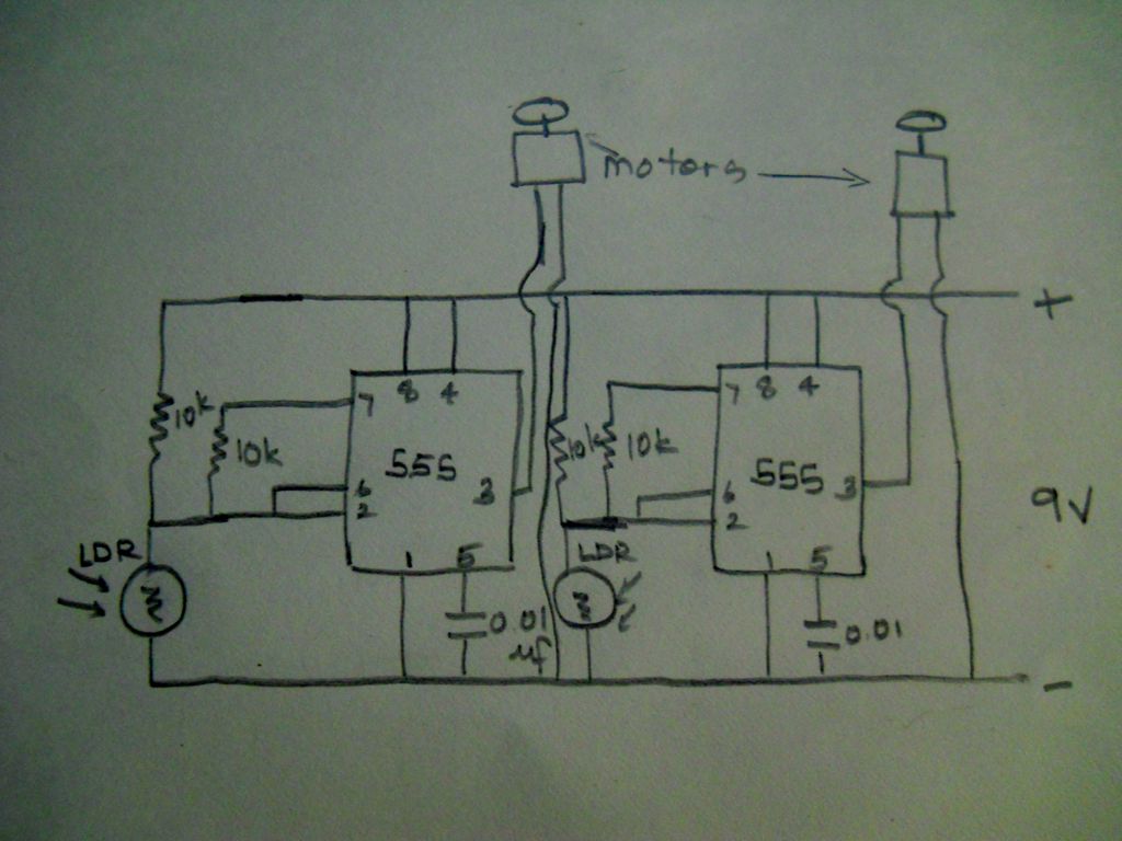
The schematic diagram of this robot is straightforward to comprehend. It is based on modifications made to a circuit from one of the reference books. The schematic for the robot features a basic structure that integrates various electronic components to...

The voltage rating of the 470 µF capacitor is not critical, provided it significantly exceeds the maximum power supply voltage, which is 12 volts in this circuit. It is essential to connect this capacitor correctly, observing its polarity. The...
An automatic power protection circuit is presented. This protection includes a step-down rectifier circuit, an overvoltage and undervoltage detection circuit, and a delay switch control circuit. The step-down circuit is responsible for the entire rectifier circuit's DC voltage. The automatic...