
555 Voltage Doubler Relay Driver

The described relay driver circuit utilizes a 555 timer IC in a Schmitt trigger configuration, which allows for robust switching characteristics and noise immunity. The circuit's design leverages the unique properties of capacitors and diodes to create a voltage doubler effect, enabling the relay to operate at a higher voltage than the supply voltage. This is particularly advantageous in applications where relay activation requires higher voltage levels, but power consumption must be minimized.
The use of a capacitor (C1) in the circuit is crucial for storing energy and providing the necessary voltage boost during relay activation. The discharge path through diode D2 ensures that the coil receives the appropriate voltage while preventing back EMF from damaging the circuit components. The choice of components, including the 555 timer, transistors, and diodes, should be made based on their voltage and current ratings to ensure reliable operation under varying load conditions.
Furthermore, the inclusion of a voltage divider allows for flexibility in input logic levels, making the circuit compatible with different control signals. This adaptability is essential in modern electronic applications where interfacing with microcontrollers or other logic devices is common.
Overall, this relay driver circuit represents a sophisticated solution for controlling relays efficiently, reducing energy waste while providing reliable operation across various applications. The design highlights the importance of careful component selection and configuration to achieve optimal performance.These novel relay driver circuits have the ability to pick up a relay with a coil voltage rating equal to double Vcc. After pickup, the relay armature is held via the application of Vcc. Under this condition, the coil power is reduced by the square of the voltage ratio, or to 25%. This is the ultimate in relay economy ”the reduction of wasted coi l power. In typical relay economy circuits, the coil power may be reduced to 25%, but the series dropping resistor dissipates an equal amount of power. In the voltage doubler relay driver, THERE IS NO SERIES RESISTOR! I believe that these voltage doubler relay driver circuits are new to the world. The versatile 555 performs this interface function well. It is configured as a Schmitt trigger inverter /driver with two outputs: Totem pole and open collector.
When output (pin 3) goes low, Q1 turns on and sources Vcc to the positive side of the coil. At the same time, the reset line (pin 7) goes low and drives the cathode of C1 to -12V. Thus the difference between the collector of Q1 and the cathode of C1 is 24V momentarily. After C1 is discharged, D2 conducts the coil current to common thus applying 12V minus one diode drop to the relay coil. When the input to the 555 goes low, pin 3 goes high, pin 7 is turned off and the relay drops. At this time C1 starts to recharge ”its charge time constant is 0. 47sec so it will be ready to fire again in about 2sec. The input logic threshold may be adjusted down to TTL levels via connecting the suggested voltage divider (R4 & R5) to pin 5 (see schematic).
This is recommended for only the CMOS TLC555 device. Otherwise, the standard bipolar 555 should work fine. This version is controlled by a high side switch contact. The switch applies Vcc directly to the relay coil. At the same time, it turns Q1 on which in turn drives the negative side of the coil to -12V. This version is controlled by a low side switch contact or perhaps a bipolar transistor or even a 2N7000 MOSFET. The switch (or transistor) grounds the negative side of the relay coil. At the same time, it turns on PNP transistor Q1 which drives the positive side of the coil to +24V via the charge stored in C1.
🔗 External reference
Related Circuits

The circuit operates at a distance of 3 feet from the oscillating pulse output of a 555 timer generating a 40kHz signal, driving a T-40-16 transducer to emit ultrasonic signals at the same frequency. The circuit is powered by...
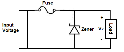
An overvoltage protection circuit is designed to safeguard electronic components from excessive voltage that could potentially cause damage or destruction. This project involves constructing a straightforward yet effective overvoltage protection circuit using a fuse and a zener diode as...

This circuit is primarily designed as a timely reminder system for monitoring individuals on duty who may fall asleep. It features a detection circuit that processes minute signals. As the LED digital electronic timing clock displays the minute, the...
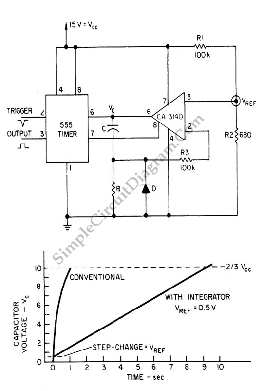
The 555 IC is a widely used component for timer circuits. By incorporating an integrator circuit, it is possible to extend the timing period of the 555 IC timer while maintaining a reasonable capacitor size. The 555 timer IC is...
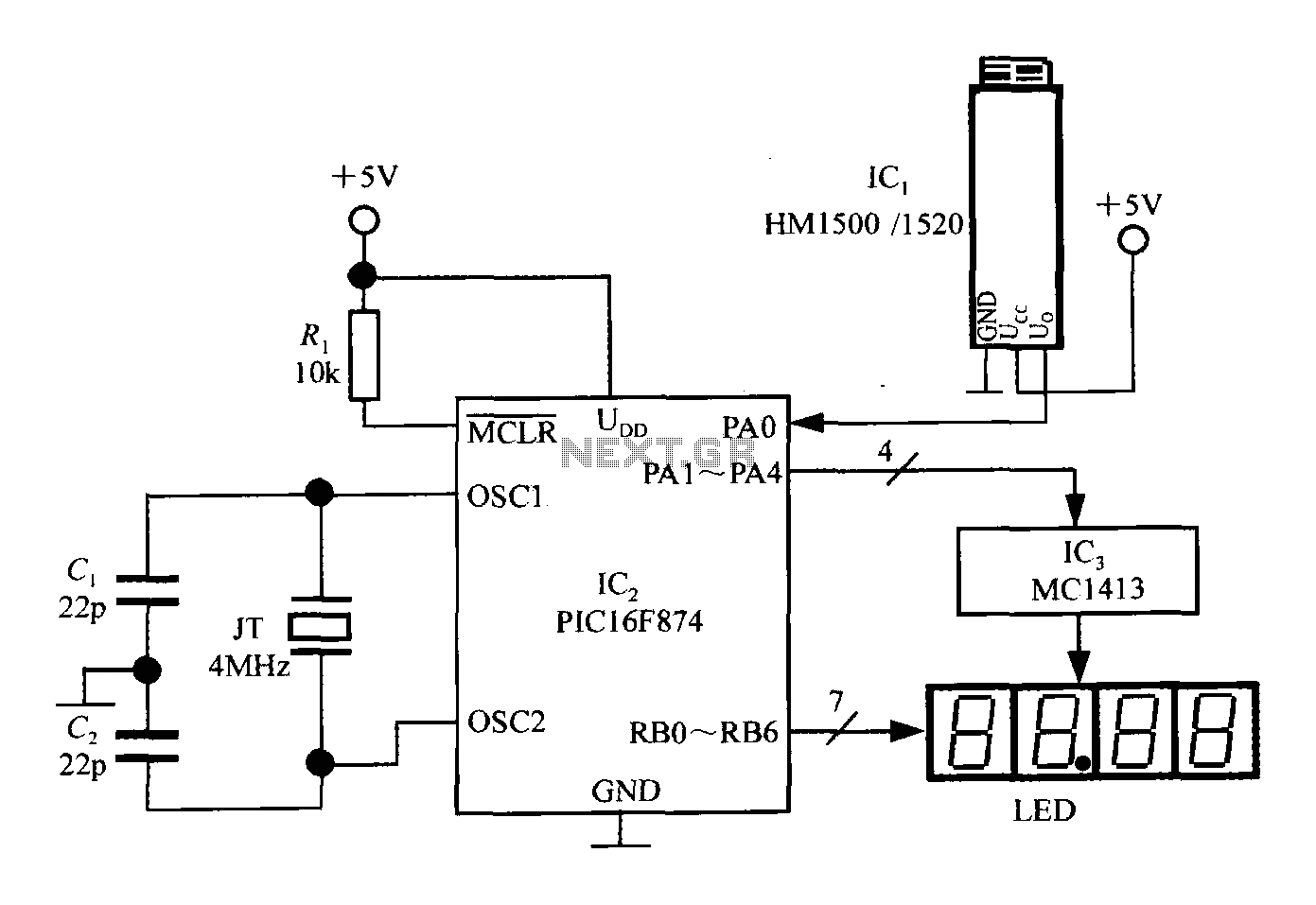
An intelligent humidity meter circuit utilizing the HM1500/1520 humidity sensor and a microcontroller configuration. The circuit operates on a +5V power supply and incorporates four common cathode LED digital displays. It employs three integrated circuits: IC1 is the HM1500/1520...
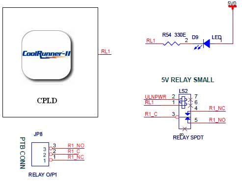
The CoolRunner-II board features external 5V relay interfacing, as indicated in the accompanying figure. The ULN2803 is utilized as a driver for the CPLD I/O lines, with the driver outputs connected to the relay modules. A PTB connector is...