
6 - 12 Volt Adjustable Power Supply Circuit Schematic Diagram
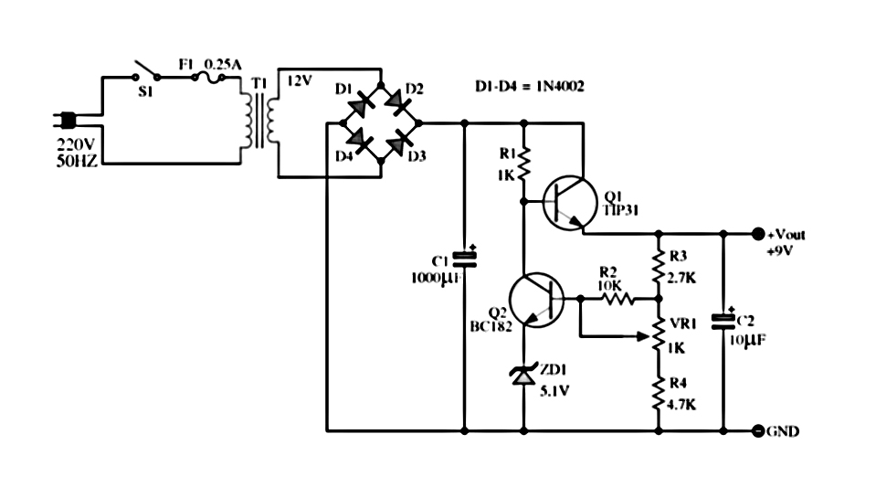
The power supply circuit operates by regulating the output voltage through a combination of transistors and resistors. The TIP31 transistor (Q1) serves as the main power regulator, allowing for efficient voltage regulation across the specified range. The second transistor (Q2) is responsible for controlling the output voltage by receiving bias from the voltage divider network formed by resistors R3, R4, and the variable resistor VR1, alongside R2. This configuration enables the user to adjust the output voltage according to their requirements.
The inclusion of the 5.1V zener diode in the circuit is critical, as it establishes a reference voltage that helps maintain a minimum output voltage. This feature is particularly important for applications that require a stable voltage supply, ensuring that the output does not fall below a specified threshold.
For assembly, the circuit can be constructed on a printed circuit board (PCB), which facilitates easy connection of components and enhances durability. The design is straightforward, making it suitable for both novice and experienced electronics enthusiasts. This adjustable power supply circuit can be utilized in various applications, including powering small electronic devices, testing circuits, and educational projects, providing versatility and practicality in its use.Power Supply in this article use a regulator that is composed of 2 pieces of NPN transistor. A transistor acts as a power regulator and a transistor again serves as a controller output voltage. Power Supply has an adjustable output with a range of 6-12 VDC. The part that serves as a power regulator is Q1 TIP31. Then the controller output voltage i s a voltage divider composed of R3, R4, VR1 and R2 provide bias to the base of Q2 to Q1 mengentrol power regulator. In a series of power supply is mounted 5. 1 V zener diode which serves to make the minimum limit the output voltage with Q2. Power Supply With transistor circuit is quite simple and can be made with the PCB holes, so for those who want to try to directly mempraktikannya.
May the power supply circuit can be useful for readers, especially for friends who need a power supply circuit with the regulator transistor. You are reading the Circuits of 6 - 12 Volt | Adjustable Power Supply Circuit And this circuit permalink url it is
🔗 External reference
Related Circuits
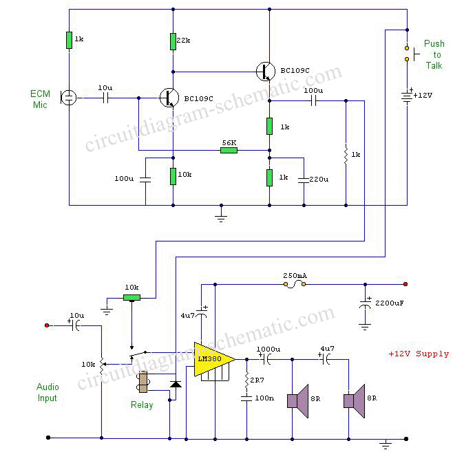
This circuit diagram represents a microphone preamplifier, specifically designed to prioritize voice signals over other audio inputs. In its basic configuration, the circuit includes a microphone unit and a change-over switch that connects to an amplifier. When the push-to-talk...
The circuit of the unit is relatively straightforward; however, setting it up can be somewhat challenging. The difficulty arises from the need for matched FETs, which are not easily obtainable. Therefore, it was essential to ensure that the circuit...
This analog switch circuit is designed to switch an analog line on or off. It consists of two analog switches in integrated circuit (IC) form that are controlled by two pushbuttons. The described analog switch circuit utilizes two integrated analog...
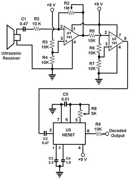
The ultrasonic receiver utilized in this circuit is specifically designed to vibrate optimally at a frequency of approximately 40 kHz. Consequently, the transmitter associated with this receiver must also emit waves at 40 kHz. When these waves interact with...
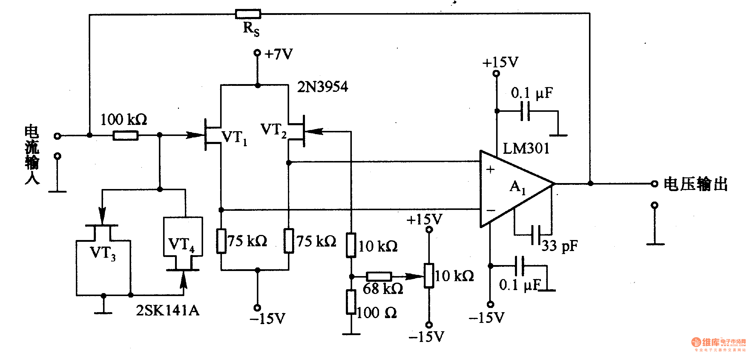
This is a low-input impedance conversion circuit with the reference resistor RS connected to the amplifier's feedback loop, resulting in an input impedance close to zero. The input current flows into the output end of the operational amplifier (Op-Amp)...
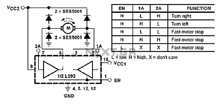
All inputs are compatible with TTL. Each output consists of a complete totem pole driver circuit, utilizing Darlington transistors and pseudo-Darlington sources. The driver enable signals, labeled as 1,2 EN and 3,4 EN, control the activation of drivers 1...