
60 LED Clock
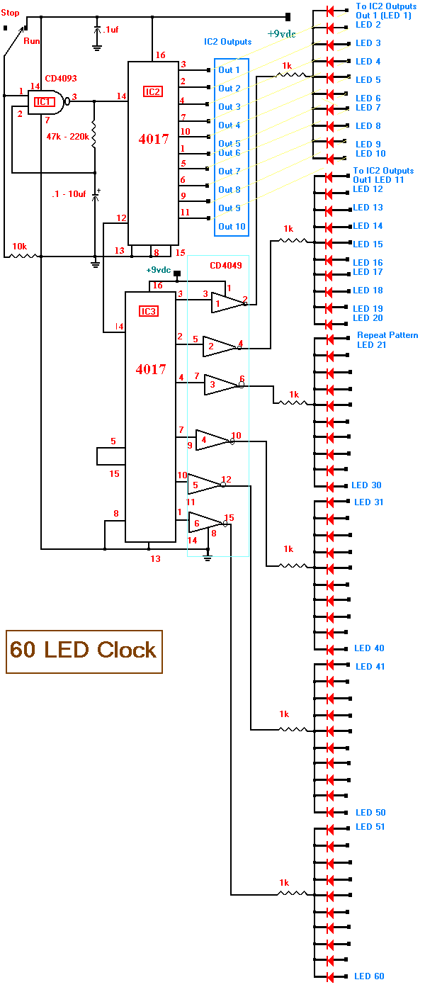
The project focuses on utilizing the CD4017 decade counter, which is a popular integrated circuit for counting applications. It counts from 0 to 10 and can be reset to zero, making it suitable for various timing and sequencing applications. The integration of the 4093 NAND gate serves as an oscillator, producing a clock signal necessary for the operation of the 4017. The clock frequency is crucial for determining how quickly the 4017 progresses through its counting sequence.
The choice of resistor and capacitor values for the 4093 is critical; the RC time constant directly influences the frequency of the output clock pulses. The relationship between the resistor (R) and capacitor (C) can be defined by the formula \( f = \frac{1}{2 \pi R C} \), where \( f \) is the frequency. Thus, a 220k ohm resistor and a 4.7µF capacitor yield a frequency of approximately 0.106 Hz, resulting in a one-second pulse.
Proper grounding of unused pins is essential to ensure stable operation. Noise introduced by floating pins can lead to erratic behavior of the circuit, particularly affecting the clock signal. Grounding the specified pins mitigates this issue, providing a more reliable performance of the 4093 NAND gate.
The operation of the circuit is straightforward. The user can switch between the STOP and RUN positions to control the counting process. In the RUN position, the 4017 will count up with each clock pulse generated by the 4093, while in the STOP position, the counting process halts. This simple yet effective design demonstrates the versatility of the 4017 chip in timing applications, providing an excellent platform for further experimentation and learning in electronics.This months project is based on the 4017 chip that we used in a project last month. If you haven`t had a chance to review the basics of the 4017 chip you may want to review the info presented in June`s project of the month. As you can see see we have changed the circuit a little. For example, the 4093 NAND gate is now set to exactly 1 second clock pulses. The clock rate is determined by the resistor and capacitor combination on the 4093. If the resistor is 220k ohms and the capacitor is 4. 7uf then the output will be 1 second clock pulses. To increase the clock rate you should decrease the value of the resistor or capacitor. To decrease the clock rate you should increase the value of the resistor or capacitor. Please remember to ground all unused legs of the 4093 or noise in the circuit will occur and cause the clock to malfunction. Therefore, ground pins 5, 6, 8, 9, 12, and 13. To operate the circuit simply move the switch from STOP to RUN. We aim to transmit more information by carrying articles. Please send us an E-mail to wanghuali@hqew. net within 15 days if we are involved in the problems of article content, copyright or other problems.
We will delete it soon. 🔗 External reference
Related Circuits
The clock described here is a simple single-digit nixie clock featuring interesting attributes without the use of complex components. It illustrates the feasibility of utilizing standard, low-voltage, general-purpose, small-signal transistors, such as the BC550, as nixie drivers. This might...
Conventionally, a MOSFET with a voltage rating of 1500V or a Half-Bridge configuration utilizing two MOSFETs rated at 800-900V is employed for Switch Mode Power Supply (SMPS) applications that require input voltages exceeding 380Vac. However, these methods present challenges,...
Upon purchasing the slave dial, it arrived without instructions, packaging, or additional details. The only visible markings, aside from decades of grime, were on the face (SMITH SECTRIC, ACELEC SYDNEY) and some markings on the bracket holding the mechanism...
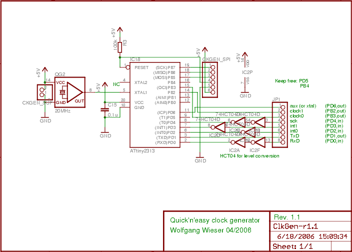
The design generates varying sampling clock write strobe pulses using an ATtiny2313 microcontroller from Atmel. For a 10MHz sampling clock, a 20MHz clock is required for the ATtiny2313, necessitating a power supply of 5V instead of 3.3V, which is...
The above shows a home-built digital clock that utilizes Nixie tubes for display. Unlike most contemporary Nixie clocks, this design does not employ transistors or integrated circuits for driving the tubes. Instead, the driving logic is constructed using neon...
This is a chronological account of a project to design and build a digital clock based on the Arduino open-source architecture, utilizing the ATMEGA8 microcontroller. The ATMEGA8 is an 8-bit, 16MHz microcontroller with integrated digital and analog inputs and...