
60watt rf radio frequency
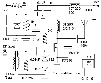
The 60 Watt RF amplifier circuit is designed for efficient amplification of radio frequency signals. The IRF840 MOSFET is the key component due to its high power handling capability and low on-resistance, which minimizes power loss during operation. The circuit operates at a supply voltage of 60V, drawing a current of 700 mA, which necessitates careful thermal management to prevent overheating of the MOSFET.
The choice of a dummy load is critical for testing the amplifier's performance. The use of a 24V 6 Watts bulb provides a manageable test load, while a 230V 60 Watts bulb can be used for higher power testing, ensuring that the amplifier can handle the desired output without distortion or damage.
The adjustment of the gate voltage is crucial for the stability and performance of the amplifier. The recommended gate voltage range of 0.8V to 1V helps to maintain the device within safe operating conditions, preventing self-oscillation that can lead to catastrophic failure.
The bifilar transformer T1 is a vital component that aids in impedance matching and signal coupling. The specific winding configuration of 8 turns of 26 SWG wire on a balun core ensures optimal performance at RF frequencies. The additional windings on the drain and the RFC contribute to the overall stability and efficiency of the amplifier, ensuring that it can operate effectively across a range of frequencies.
This amplifier design is suitable for various applications in RF transmission and can be integrated into more complex systems requiring RF signal amplification. Proper assembly and tuning of the circuit, along with adherence to the specified parameters, will yield reliable performance and longevity of the amplifier.The 60Watt RF (Radio Frequency) Amplifier is simple all solid accompaniment ambit application ability mosfet IRF840. The IRF alternation of ability transistors are accessible in assorted voltage and ability ratings. A distinct IRF840 can handle best ability achievement of 125 watts. Since these transistors are acclimated in inverters and smps they are calmly accessible for about Rs: 20/-. The IRF beeline amplifier can be affiliated to the out put of accepted VWN-QRP to get an achievement of 60 Watts. The ambit draws 700 ma at 60 Volt Vcc. Good calefaction bore is a charge for the ability transistor. Alignment of the ambit is actual easy. Connect a copy amount to the out put of the circuit. You can use some baby ball like 24V 6Watts as the copy load. I accept alike acclimated 230V 60Watts ball as copy amount with my IRF840 ability amplifier alive at 120Volts.
Adjust the 10K preset to get about 100 ma Cesspool current. I acclimated aboideau voltage of 0. 8V with my beeline amplifier. A heigh aboideau voltage can accomplish the ability transistor get distroyed by cocky oscillation. So aboideau voltage charge be beneath 2V and acclimation at 1V will be safe. Bifalar transformaer T1 is anguish with 8 turns 26SWG on 1. 4 x 1 balun core. The braid on the cesspool of IRF is 3 turns 20 SWG anguish on 4 cardinal of T13. 9 torroids (two torroids are ample to anatomy a balun core). The RFC at the Vcc band is 20 Turns 20 SWG anguish on T20 torroid. 🔗 External reference
Related Circuits
Spikes in the center of a sawtooth wave are eliminated in this circuit by triggering at specific intervals. This circuit is designed to mitigate unwanted spikes that occur in the center of a sawtooth waveform. The sawtooth wave, characterized by...
This circuit will produce over +10 dBm in the 1800-3000 MHz range. Drive power is 7 dBm in the 900 to 1500 MHz range. The PC board is G-10 epoxy double-sided. Artwork is shown above, as well as parts...
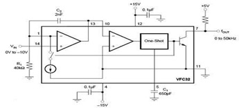
The circuit diagram of a voltage-to-frequency (V/F) converter is presented, designed to handle negative input voltage. It employs the VFC32 voltage-to-frequency converter, which is commonly utilized in various applications. The V/F converter circuit is essential in converting an analog voltage...
2012 Honda Odyssey Radio Wiring Diagram Manual PDF Download. The 2012 Honda Odyssey Radio Wiring Diagram Manual provides a detailed schematic of the audio system's wiring configuration for the vehicle. This manual is essential for understanding the connections and functionalities...
The circuit utilizes the principle that the forward voltage of a silicon diode changes in a relatively linear manner with temperature when supplied by a constant current source. Diode D1 and resistor R2 create a potential divider connected to...
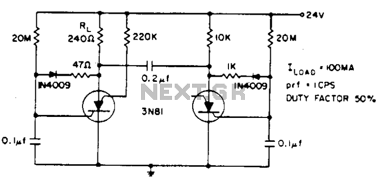
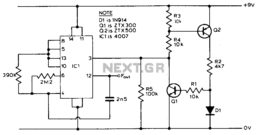
Electrolytic capacitors are not required to generate a 1 cps frequency. When the silicon-controlled switch (SCS) is triggered, the 0.2 µF commutating capacitor deactivates the other capacitor and charges its gate capacitor to a negative potential. The gate capacitor...