
Gasfet Frequency Doubler
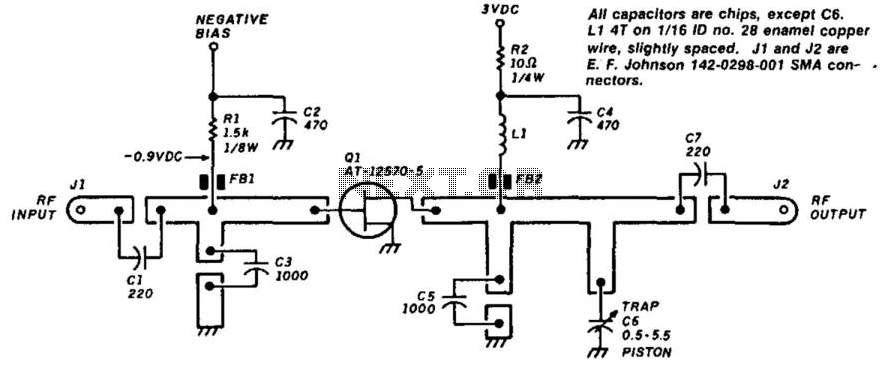
The described circuit is designed for operation within the frequency range of 1800 to 3000 MHz, achieving an output power level exceeding +10 dBm. It utilizes a drive power of 7 dBm, specifically optimized for the lower frequency range of 900 to 1500 MHz. The circuit is implemented on a G-10 epoxy double-sided printed circuit board (PCB), which is known for its durability and thermal stability, making it suitable for high-frequency applications.
The PCB layout is critical for performance at these frequencies; hence, the artwork and parts placement must be meticulously designed to minimize signal loss and maintain impedance matching throughout the circuit. It is recommended to use connectors that are appropriate for these frequency ranges, such as SMA connectors, which provide reliable connections with minimal signal degradation.
For proper operation, the circuit requires a negative bias supply that can be adjusted between 0 to 3 V. This biasing is essential for the active components within the circuit, influencing their operating points and overall performance. Careful consideration should be given to the power supply design to ensure low noise and stability, which are crucial for maintaining signal integrity in high-frequency applications.
Overall, this circuit is suitable for applications requiring amplification and signal processing within the specified frequency ranges, making it a valuable component in RF communication systems. This circuit will produce over +10 dBm in the 1800-3 000-MHz range. Drive power is 7 dBm in the 900-to-l 500-MHz r ange. The PC board is G-10 Epoxy doublesided. Artwork is shown above, as well as parts placement connectors suitable for these frequencies (such as SMA) should be used. A negative bias supply of 0 to 3 V is required. 🔗 External reference
Related Circuits
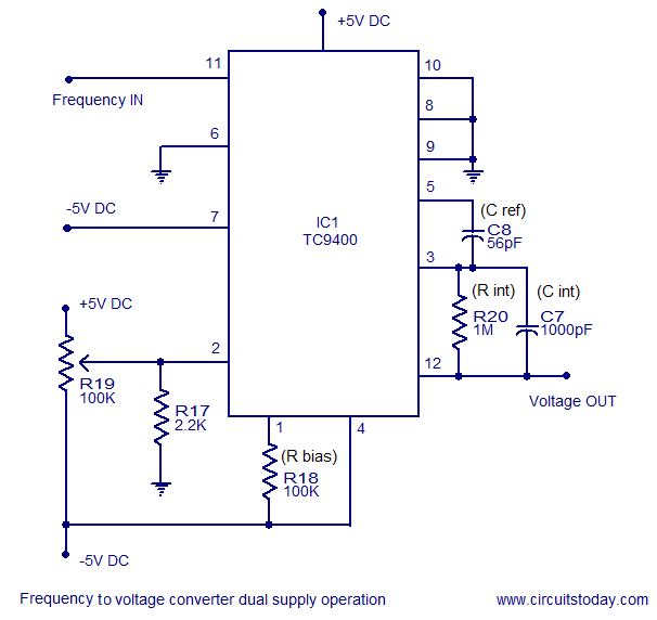
A simple frequency to voltage converter circuit designed around the TC9400 F to V / V to F converter IC. Dual and single supply versions are provided. The TC9400 is a versatile integrated circuit that converts frequency signals into corresponding...
All miniature electronic devices operate off batteries. Some of them require higher than the standard battery voltages to function efficiently. Miniature electronic devices, which include a wide range of applications from portable gadgets to remote sensors, typically rely on battery...
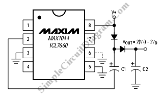
This is a simple circuit of a Positive Voltage Doubler. This circuit utilizes the MAX1044/ICL7660. The Schottky diode was selected to reduce the voltage drop. The Positive Voltage Doubler circuit is designed to convert a lower input voltage into a...
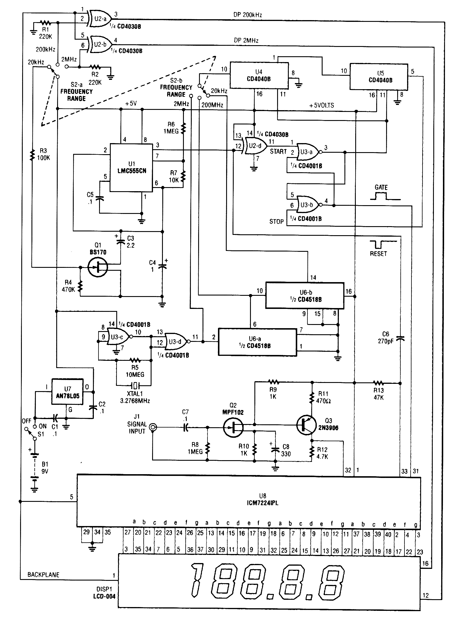
This is a schematic and block diagram of a 2-MHz frequency counter. It employs an LSI counter/display driver, an LCD readout, and several logic chips for timebase and timing pulse circuitry. Transistors Q2 and Q3 form a signal input...
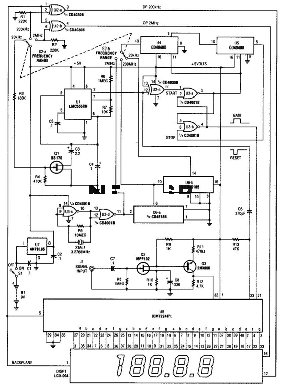
This is a schematic and block diagram of a 2-MHz frequency counter. It utilizes an LSI counter/display driver, an LCD readout, and several logic chips for timebase and timing pulse circuitry. Q2 and Q3 serve as a signal (input)...
%2Bdecoder%2BCircuit%2Bschematic%2Busing%2BM8870.png)
This DTMF (Dual Tone Multi Frequency) decoder circuit identifies the dial tone from the telephone line and decodes the key pressed on the remote telephone. For the detection of DTMF signaling, the IC MT8870DE, a touch tone decoder IC,...