
Temperature-to-frequency converter
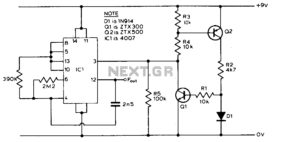
The described circuit is an innovative temperature sensor that leverages the temperature-dependent characteristics of a silicon diode to provide a variable frequency output. The constant current source provides a stable reference, ensuring that the diode operates in its forward bias region. As the temperature increases, the forward voltage drop across diode D1 decreases due to the negative temperature coefficient of the diode. This change influences the base-emitter voltage of transistor Q1, leading to a reduction in its conduction state.
The potential divider formed by R2 and D1 is crucial for determining the operational point of Q1. As the temperature rises and the forward voltage of D1 decreases, the voltage drop across R2 increases, which in turn raises the output voltage from Q1. This output acts as a control signal for the CMOS VCO, which is designed to produce a frequency that varies with the control voltage. The linear relationship between temperature and frequency is particularly useful for applications requiring precise temperature measurement and control.
The circuit's performance, characterized by an increase of approximately 3 Hz per degree Celsius, indicates a well-calibrated response over the specified temperature range of 0 °C to 60 °C. At the lower temperature limit, the output frequency is established at 470 Hz, providing a clear and measurable output that can be utilized in various electronic applications, including temperature monitoring systems and feedback control loops. The design emphasizes simplicity and efficiency, making it suitable for integration into compact electronic devices where space and power conservation are critical.The circuit exploits the fact that when fed from a constant current source, the forward voltage of a silicon diode varies with temperature in a reasonably linear way. Diode Dl and resistor R2 form a potential divider fed from the constant current source. As the temperature rises, the forward voltage of Dl falls tending to turn Ql off. The output voltage from Ql will thus rise, and this is used as the control voltage for the CMOS VCO With the values shown, the device gave an increase of just under 3 Hz/°C (between 0 °C and 60 °C) giving a frequency of 470 Hz at 0 °C. 🔗 External reference
Related Circuits
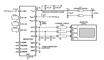
This digital-to-analog converter (DAC) integrated circuit is designed for optimal noise performance, minimizing both radiated and conducted noise. A recommended connection diagram for the ADV7123 is depicted in the following schematic diagram. According to the ADV7123 datasheet, this device...
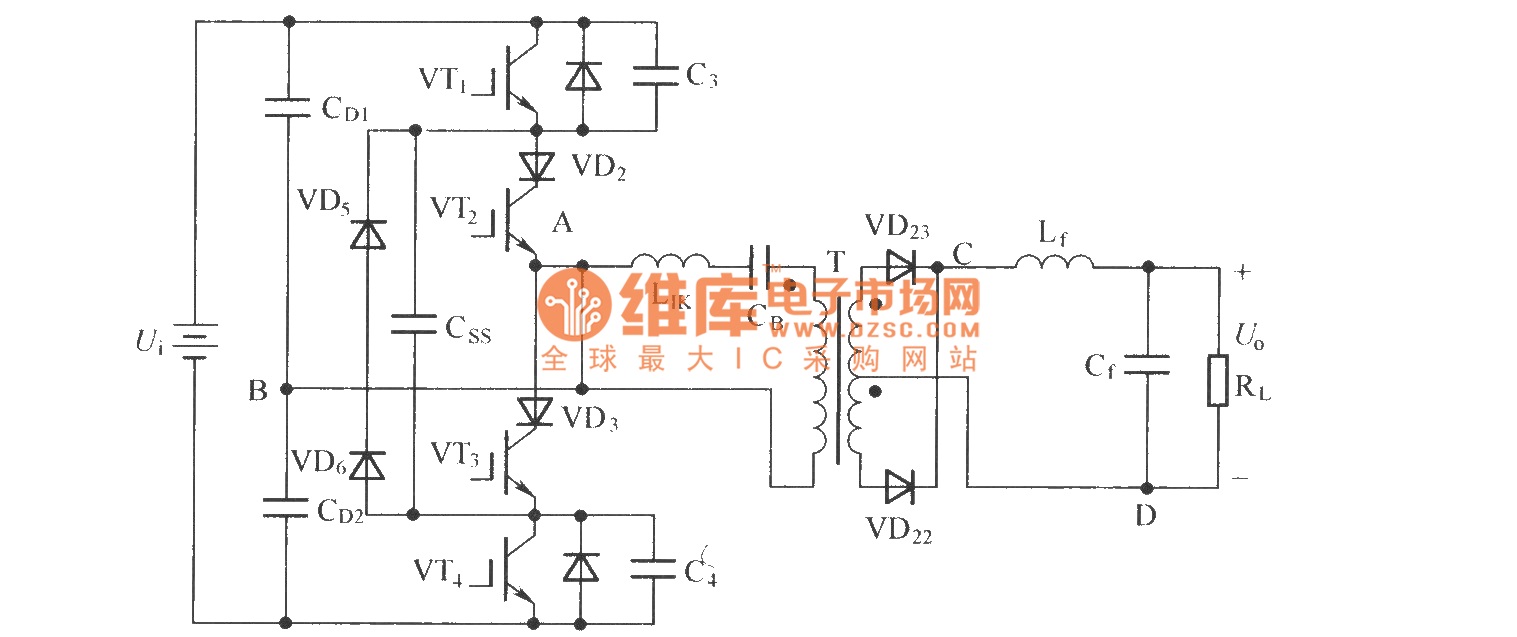
To eliminate circulating current in a zero-voltage switch three-level DC converter during its zero state, a zero-voltage zero-current switch three-level DC converter circuit has been proposed. The primary distinction between this circuit and the standard zero-voltage switch three-level DC...
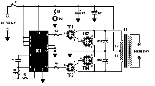
The final power transistors TR2 and TR4 must be mounted on appropriately sized heatsinks to prevent overheating. Suitable options include MJ4033, MJ3007, or other NPN transistors. The maximum power output is dependent on the transformer T1's core size. For...
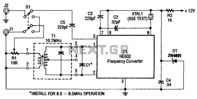
A Signetics NE602 is utilized in this converter to tune the frequency range of 9.5 to 9.8 MHz. An AM car radio functions as a tunable intermediate frequency (IF) amplifier, with the output being taken from J2, the auto...

This power converter is utilized in the LHC machine to supply power to superconducting magnets. It is situated within the underground installation of the LHC, positioned close to the loads to minimize cable losses. The converter operates at a...
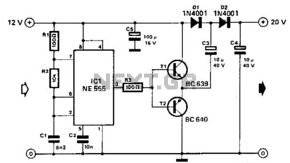
Using a 555 timer and voltage doubler, this circuit will supply over 50 mA at 20 V DC. Transistors T1 and T2 act as power amplifiers to drive the voltage doubler. The frequency of operation is approximately 8.5 kHz. The...