
65W notebook laptop power adapter circuit
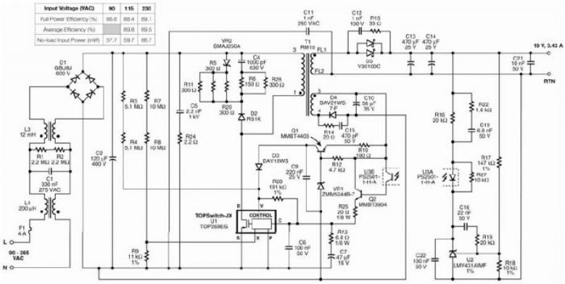
The circuit design employing the TOP269EG IC is characterized by its efficiency and simplicity, making it suitable for notebook laptop power adapters. The flyback topology allows for isolation between the input and output, enhancing safety and reliability. The integrated MOSFET reduces component count and simplifies the layout, which is advantageous for compact designs.
The common-mode inductors L3 and L4 are critical for minimizing electromagnetic interference (EMI), ensuring compliance with regulatory standards. The X class capacitor C1 plays a vital role in filtering high-frequency noise, while resistors R1 and R2 are essential for safety, providing a discharge path for C1 to prevent electric shock hazards. The bridge rectifier D1 is responsible for converting the AC voltage from the mains to a usable DC voltage, which is then smoothed by bulk capacitor C2, ensuring stable operation of the power supply.
Capacitor C7's function in the auto-restart feature is crucial for maintaining continuous operation. Upon initial power-up, C7 charges, allowing the IC to begin switching. In the event of an output overvoltage condition, the feedback mechanism involving VR1 and Q1 ensures that the system can safely shut down to prevent damage to the connected load. This feedback loop not only protects the power adapter but also enhances the overall reliability of the power supply system.
In summary, the design utilizing the TOP269EG IC in a flyback configuration provides a robust solution for power conversion in notebook laptops, combining safety features, efficient regulation, and compactness into a single integrated circuit solution.Using TOP269EG off-line switcher IC, (U1), in a flyback configuration can be designed a very simple high efficiency notebok laptop power adapter. TOP269EG IC has an integrated 725 V MOSFET and a multi-mode controller. It regulates the output by adjusting the MOSFET duty cycle, based on the current fed into its CONTROL pin.
Common-mode inductors L3
and L4 provide filtering on the AC input. X class capacitor C1 provides differential filtering, and resistors R1 and R2 provide safety from shock if the AC is removed, by ensuring a path for C1 to discharge. This is required by safety agencies when the capacitor value exceeds 100 nF. Bridge rectifier D1 rectifies the AC input, and bulk capacitor C2 filters the DC. Capacitor C7 provides the auto-restart timing for U1. At startup this capacitor is charged through the DRAIN (D) pin. Once it is charged U1 begins to switch. Capacitor C7 stores U1 utilizes an output overvoltage shutdown function. An increase in output voltage causes an increase in the bias winding on the primary side, sensed by VR1.
A sufficient rise in the bias voltage causes VR1 to conduct and bias Q1 to inject current into the Voltage Monitor (V) pin of U1. When the current exceeds 336 uA, U1 enters the overvoltage shutdown mode and latches off.
Related Circuits
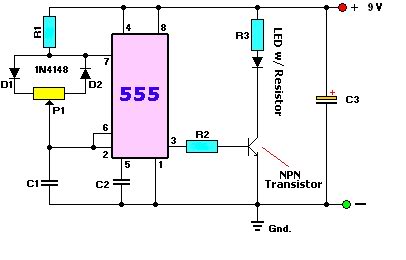
A user is new to the forum and has limited experience in DIY electronics. The current project involves creating a battery-powered LED dimmer circuit. The objective of the project is to design a battery-operated LED dimmer circuit that allows for...
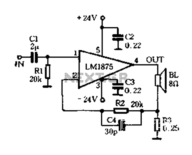
A current-sense amplifier is utilized to enhance the performance of the LM1875 current-mode amplifier circuit, as depicted in Figure 5-20. The resistor R3 and the series resistance of the speaker contribute to the current flowing through R3. This current...
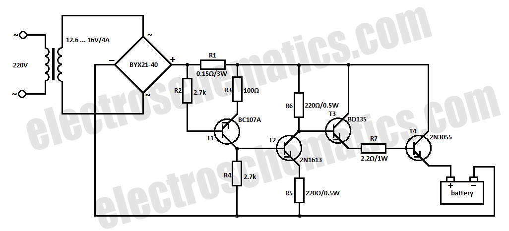
The car battery charging current is automatically limited to 4.2A. If there is a 600mV voltage on R1 (indicating 4A flowing through it), the T1 transistor begins to conduct. This prevents excessive charging current as the base current of...
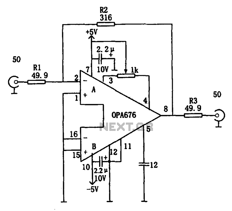
The circuit features a broadband video amplifier with a 50-ohm input/output impedance. To ensure optimal signal transmission and minimize reflected signals, it is often necessary to match the input and output impedances of the amplifier. The broadband video amplifier...
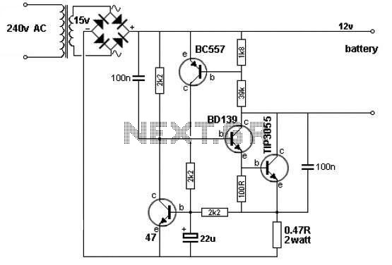
A simple 12V battery charger circuit can be designed using a TIP3055 power transistor to limit the current to the battery. The circuit turns off when the battery voltage reaches approximately 14V or if the current exceeds 2A. This...
The primary objective is to present the circuit diagram and describe the software utilized. A UDP application is employed to transmit commands to the microcontroller, which subsequently activates or deactivates the relay. It is anticipated that TCP implementation could...
Warning: include(partials/cookie-banner.php): Failed to open stream: Permission denied in /var/www/html/nextgr/view-circuit.php on line 713
Warning: include(): Failed opening 'partials/cookie-banner.php' for inclusion (include_path='.:/usr/share/php') in /var/www/html/nextgr/view-circuit.php on line 713