
A/D Board

The circuit design facilitates the integration of two 12-bit Analog-to-Digital (A/D) converters with an IBM PC using the printer port, which is a common interface for older computer systems. The converters' operation is based on a serial output configuration that utilizes just two of the available data lines from the printer port, specifically DATA A OUT and DATA B OUT. This allows for efficient data transmission while conserving the limited resources of the printer port.
Since the printer port does not provide power, an essential aspect of the design involves the interface software, which is programmed to set the remaining six data lines to a high state. This action effectively supplies the necessary power to the digital components of the A/D converters. It is important to note that these converters are equipped with internal optoisolators; thus, isolated power supplies must be provided for the analog sections to ensure proper functionality and prevent any potential damage from ground loops or other electrical interference.
The A/D converters are capable of executing 12-bit conversions in a rapid timeframe of 6 microseconds under optimal conditions. However, due to the constraints of the software-driven approach employed in this design, the conversion period is extended to around 100 microseconds, which can vary based on the clock speed of the IBM PC. This trade-off between speed and the simplicity of the software implementation is a key consideration in the overall design.
To achieve synchronous operation of the A/D converters, the circuit design cleverly utilizes the optoisolator inputs, connecting the clock and start inputs in series. This arrangement allows both converters to operate in harmony, ensuring that data conversion occurs simultaneously. The accompanying software plays a critical role in managing the entire conversion process. It is responsible for initiating conversions, generating the necessary clock pulses, and reading the output data bits as they become available. The collected data is subsequently stored in the PC's memory for further processing or analysis.
Overall, this design exemplifies a practical application of interfacing A/D converters with a legacy computing platform, highlighting the importance of careful consideration in power management, timing control, and data handling in electronic circuit design. An IBM PC can operate the two 12-bit A/D converters in Fig. 1 via its printer port. The converters" serial outputs use only two o f the printer port"s eight data lines (DATA A OUT, DATA B OUT). Because the IBM PC"s printer port supplies no power, interface software running on the PC programs the six unused data lines high. Busing these data lines provides power for the digital portion of the A/D converters. (The converters have internal optoisolators. Consequently, you must provide isolated supplies for their analog sides.) Although the converters can execute 12-bit conversions in 6 /as, the slow software-driven approach used in this Design Idea stretches conversion periods out to about 100 /is (depending on your PC"s clock speed).
The circuit takes advantage of the converters" optoisolator inputs to put their clock and start inputs in series. Therefore, the converters operate synchronously. The accompanying software starts the conversions, issues clock pulses, reads the data bits as they become available, and stores them in memory.
Related Circuits
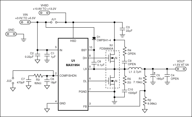
This document outlines the layout considerations for switch-mode DC-DC converter printed circuit boards (PCBs) aimed at minimizing switching noise and electromagnetic interference (EMI). The layout of switch-mode DC-DC converter PCBs is critical in ensuring efficient operation and compliance with electromagnetic...
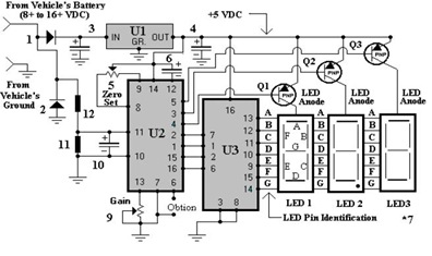
To create a dashboard digital voltmeter circuit diagram that includes a parts list, PCB layout, and component placement, a full PDF article is available for download. The dashboard digital voltmeter circuit is designed to provide an accurate measurement of voltage...
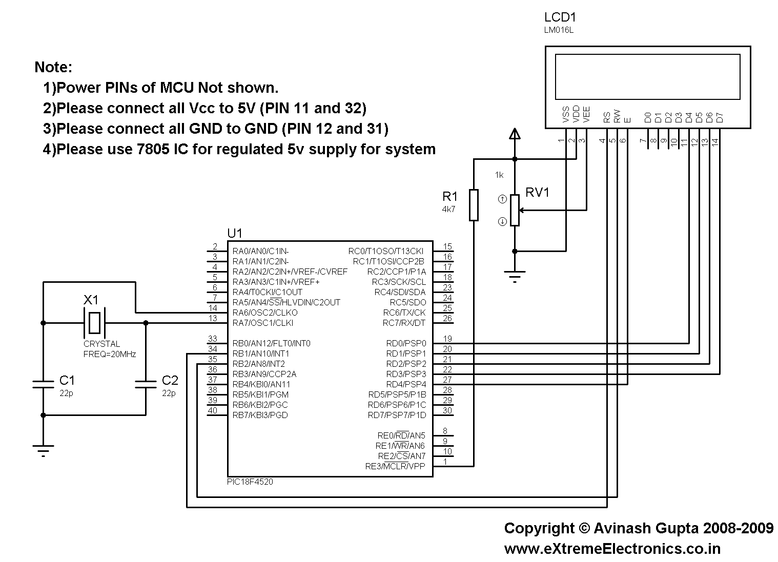
This is a practical expansion board designed for a PIC development board, intended for DIY use with a 16x2 alphanumeric LCD. The expansion board connects to the PIC development board, providing LCD support, which is essential for numerous projects...
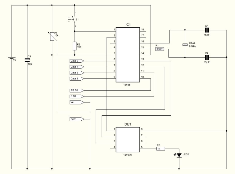
The program loaded in the 12F675 device which has no osccal value will force a pulse on GPIO.4 and it will make a loop while increasing the osccal value internally. GPIO.5 will send the current osccal value used for...
The enable signal for the USB chip and GLCD controller is generated by a PLD decoder from the address lines. The memory map for the I/O of the 8051SBC board indicates that the available space ranges from 0x0300 to...
CPU NatSemi Geode operating at frequencies of 200/233/266/300 MHz (with a default speed of 233 MHz on-board) or refer to the Geode link. The VGA/LCD interface is NS GX5530, featuring shared memory of 2.5MB, supporting CRT displays and 18-bit...