
A typical liquid crystal display inverter circuit OZ965
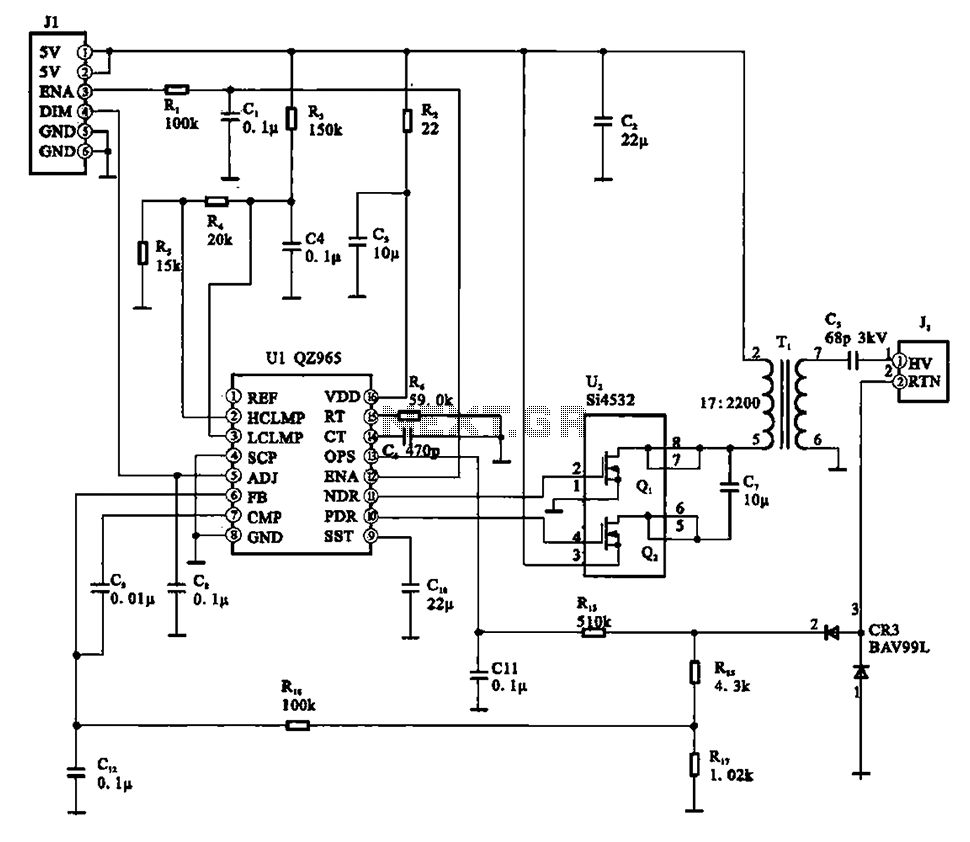
The liquid crystal display inverter circuit utilizing the OZ965 chip is designed to efficiently convert low voltage DC into high voltage AC, suitable for powering the backlight of LCD panels. The circuit begins with a 5V DC input supplied to the OZ965 control chip via pin J1, which is responsible for regulating the operation of the entire circuit.
Capacitor C2 plays a crucial role in filtering the input voltage to ensure a stable supply to the field effect transistor (U1). This transistor acts as a switch that modulates the current flowing into the step-up transformer. The transformer is essential for elevating the voltage from the low 5V level to the required high voltage, which is necessary for the operation of the backlight lamps.
The enable control signal (ENA) is sent to the OZ965 chip, indicating that the inverter circuit should begin operation. Upon activation, the chip generates two PWM signals at the output pin U1, which are 180 degrees out of phase. These signals drive the field effect transistor (U1) in a manner that allows for efficient energy transfer to the step-up transformer.
As a result of this operation, the transformer steps up the voltage significantly, reaching approximately 800V. This high voltage is then delivered to the backlight lamp socket, effectively illuminating the LCD panel. The design of this inverter circuit exemplifies a compact and efficient solution for powering LCD backlights, utilizing a combination of modern semiconductor technology and traditional transformer principles. The overall configuration ensures reliable performance and longevity of the backlight system in various display applications.A typical liquid crystal display inverter circuit (OZ965) It shows a typical liquid crystal display of the inverter circuit, which is mainly controlled by the 02965 chip, the d riving field effect transistor U2, step-up transformer, the backlight socket part and associated circuitry configured. After 5v DC voltage by the control chip UI widget Jl provided (02 965) of the pin DC voltage; at the same time, by filtering electrical pit C2 after driving to a field effect transistor Ul step-up transformer and power supply; enable control signal (ENA) through plug Jl feet into the control chip, after the inverter circuit starts from the Ul feet pin output two opposite phase PWM pulse signal, the drive field effect transistor Ul put into large after the step-up transformer, the rise the pulse voltage transformer voltage up to about 800V, by backlight backlight lamp socket to power.
Related Circuits
The schematic closely resembles the one found in the CPLD Development Board Tutorial, as it is essentially the same board with a minor addition. The new components are located in the lower right corner, including eight DIP switches, a...
An article previously discussed connecting to the Raspberry Pi board from a Linux PC using the serial port. This time, the focus is on how to achieve the same connection using a Windows PC. In this case, a Windows...
The circuit depicted in Figure 7-32 is designed for an excitation device capable of handling a terminal voltage of 400V and a capacity of less than 75kW for synchronous generator motors, enabling automatic adjustment of excitation. When the generator...
This light dimmer control features active timing capacitor reset or AC line zero-crossing synchronization. The 13 additional components are common and cost less than $2. Performance at the low end is exceptionally smooth and snap-free, even better than the...
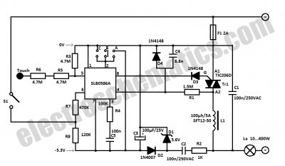
The bi-directional sequencer employs a 4-bit binary up/down counter (CD4516) and two "1 of 8 line decoders" (74HC138 or 74HCT138) to create the well-known "Night Rider" display. A Schmitt Trigger oscillator generates the clock signal for the counter, with...
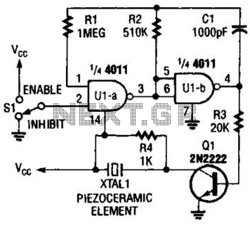
A CMOS gate and transistor buffer can be used as an effective driver for a piezoelectric transducer. The use of a CMOS gate combined with a transistor buffer offers a robust solution for driving piezoelectric transducers. CMOS technology, known for...