
A709 a voltage follower circuit diagram
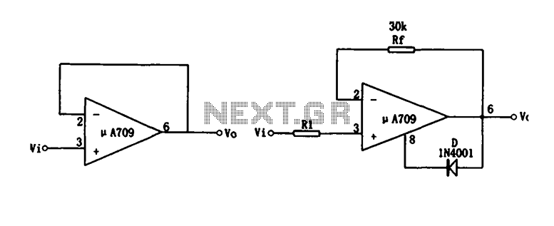
The voltage follower circuit, also known as a unity gain buffer, is characterized by its ability to provide high input impedance and low output impedance. This feature is particularly advantageous in applications where signal integrity must be maintained during transmission, as it prevents loading effects on the preceding stage. The operational amplifier's configuration allows it to replicate the input voltage at the output, ensuring that the output follows the input without amplification.
In practical applications, the voltage follower is frequently used in sensor interfaces, where the signal from a sensor must be buffered before being sent to an analog-to-digital converter (ADC) or further processing stages. The high input impedance ensures that the sensor's output is not significantly affected by the circuit's loading, preserving the accuracy of the measurement.
In the context of the operational amplifier's performance, the stability of the circuit is paramount. The presence of strong negative feedback enhances the linearity and reduces distortion, making the voltage follower suitable for high-fidelity applications. However, care must be taken to avoid conditions that could lead to instability, such as excessive input signal amplitudes that approach the power supply limits of the operational amplifier. In such cases, the circuit may enter a state of saturation, resulting in a loss of linearity and potential distortion of the output signal.
To prevent instability caused by internal oscillations, additional components such as compensating capacitors or resistors may be introduced in the feedback path. These components can help to stabilize the operational amplifier's response, ensuring consistent performance across a range of operating conditions. Additionally, selecting operational amplifiers with suitable bandwidth and slew rate specifications is critical to maintaining the desired performance characteristics in voltage follower applications.Figure (a) shows the circuit as a voltage follower, it is a special case of the in-phase amplifying circuit, the input signal from the integrated operational amplifier with the end of the introduction phase, the feedback resistor is zero, negative feedback is very strong, very stable op amp input impedance great. Output resistance is very small, so this circuit has an impedance conversion function. Impedance transformation means effect the so-called after amplifying a voltage follower, the output voltage is approximately equal to the electromotive force and the output signal source resistance is small.
The circuit is used as an input stage, an intermediate buffer stage and an output stage. The basic relationship of the circuit as follows: Vi + Vis Vo Vo -AVis Where: A-- the open-loop voltage amplification factor; Vis-- pure op amp input voltage; This circuit, when the voltage of the input signal amplitude is increased to nearly the op amps positive supply voltage, the deadlock may occur that will not be the normal output signal, which is due to the positive feedback op amp internal parasitic oscillations produced. In order to prevent this phenomenon, may be employed in Fig (b)
Related Circuits
Check the three-phase motor with broken bars as shown in the inspection circuit for the three-phase motor with broken bars. The inspection circuit for a three-phase motor with broken bars is designed to diagnose and evaluate the condition of the...
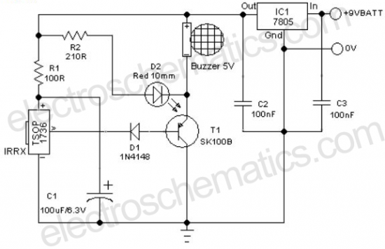
A remote-controlled alarm circuit utilizing the TSOP1736. This circuit involves routing an electric cable to connect a calling bell switch near the bed of an elderly individual. The remote-controlled alarm circuit designed with the TSOP1736 is an innovative solution for...
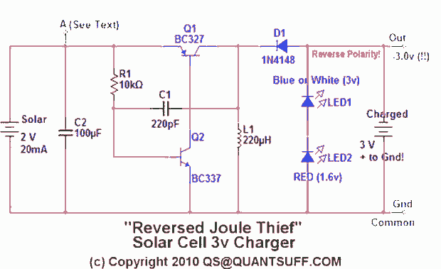
This design presents an innovative approach to the Joule Thief (JT) circuit typically utilized in garden lights. Instead of directly charging a 1.2V battery from the solar cell and converting the power to operate a 3-volt LED, this circuit...
The circuit utilizes an integrated Hall effect sensor for an AC motor control system. It operates by detecting the presence of magnets or other magnetic objects near the Hall IC element of the induction motor. This configuration functions as...
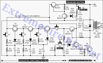
This intelligent electronic lock circuit is constructed using only transistors. To unlock this electronic lock, the user must press tactile switches S1 through S4 in sequence. For added security, these switches can be labeled with different numbers on the...
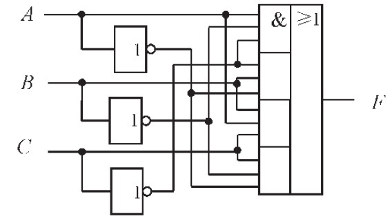
The design of the combinational logic circuit is diverse. An example chosen for detailed explanation is the implementation of an even parity check circuit. The parity check circuit exhibits particular characteristics and practicality in the analysis and design of...
Warning: include(partials/cookie-banner.php): Failed to open stream: Permission denied in /var/www/html/nextgr/view-circuit.php on line 713
Warning: include(): Failed opening 'partials/cookie-banner.php' for inclusion (include_path='.:/usr/share/php') in /var/www/html/nextgr/view-circuit.php on line 713