
Light circuit diagram: Intelligent Electronic Lock

The operation of this electronic lock circuit relies heavily on the precise timing and sequence of the switch activations. The design ensures that unauthorized access is thwarted by requiring a specific sequence and timing for the password entry, while the disabling feature adds an additional layer of security by temporarily rendering the system inactive upon any unauthorized attempt. The use of transistors in this design not only simplifies the circuit but also enhances its reliability by reducing the number of components needed. The careful selection of resistors and capacitors allows for fine-tuning of the timing characteristics, ensuring the system is both responsive and secure. The integration of zener diodes for voltage regulation plays a crucial role in maintaining the stability of the circuit during operation, particularly in the disabling section, where it prevents false triggering due to voltage fluctuations. Overall, this electronic lock circuit is designed to provide a robust solution for secure access control, combining ease of use for authorized users with effective deterrents against unauthorized attempts.This intelligent electronic lock circuit is built using transistors only. To open this electronic lock, one has to press tactile switches S1 through S4 sequentially. For deception you may annotate these switches with different numbers on the control panel/keypad. For example, if you want to use ten switches on the keypad marked 0` through 9`, use any four arbitrary numbers out of these for switches S1 through S4, and the remaining six numbers may be annotated on the leftover six switches, which may be wired in parallel to disable switch S6 (shown in the figure). When four password digits in 0` through 9` are mixed with the remaining six digits connected across disable switch terminals, energisation of relay RL1 by unauthorised person is prevented.
For authorised persons, a 4-digit password number is easy to remember. To energise relay RL1, one has to press switches S1 through S4 sequentially within six seconds, making sure that each of the switch is kept depressed for a duration of 0. 75 second to 1. 25 seconds. The relay will not operate if on` time duration of each tactile switch (S1 through S4) is less than 0.
75 second or more than 1. 25 seconds. This would amount to rejection of the code. A special feature of this circuit is that pressing of any switch wired across disable switch (S6) will lead to disabling of the whole electronic lock circuit for about one minute. Even if one enters the correct 4-digit password number within one minute after a disable` operation, relay RL1 won`t get energised.
So if any unauthorised person keeps trying different permutations of numbers in quick successions for energisation of relay RL1, he is not likely to succeed. To that extent, this electronic lock circuit is fool-proof. This electronic lock circuit comprises disabling, sequential switching, and relay latch-up sections. The disabling section comprises zener diode ZD5 and transistors T1 and T2. Its function is to cut off positive supply to sequential switching and relay latch-up sections for one minute when disable switch S6 (or any other switch shunted across its terminal) is momentarily pressed.
During idle state, capacitor C1 is in discharged condition and the voltage across it is less than 4. 7 volts. Thus zener diode ZD5 and transistor T1 are in non-conduction state. As a result, the collector voltage of transistor T1 is sufficiently high to forward bias transistor T2. Consequently, +12V is extended to sequential switching and relay latch-up sections. When disable switch is momentarily depressed, capacitor C1 charges up through resistor R1 and the voltage available across C1 becomes greater than 4.
7 volts. Thus zener diode ZD5 and transistor T1 start conducting and the collector voltage of transistor T1 is pulled low. As a result, transistor T2 stops conducting and thus cuts off positive supply voltage to sequential switching and relay latch-up sections.
Thereafter, capacitor C1 starts discharging slowly through zener diode D1 and transistor T1. It takes approximately one minute to discharge to a sufficiently low level to cut-off transistor T1, and switch on transistor T2, for resuming supply to sequential switching and relay latch-up sections; and until then the circuit does not accept any code. The sequential switching section comprises transistors T3 through T5, zener diodes ZD1 through ZD3, tactile switches S1 through S4, and timing capacitors C2 through C4.
In this three-stage electronic switch, the three transistors are connected in series to extend positive voltage available at the emitter of transistor T2 to the relay latch-up circuit for energising relay RL1. When tactile switches S1 through S3 are activated, timing capacitors C2, C3, and C4 are charged through resistors R3, R5, and R7, respectively.
Timing capacitor C2 is discharged through resistor R4, zener diode ZD1, and transistor T3; timing capacitor C3 through resistor R6, zener diode ZD2, and transis 🔗 External reference
Related Circuits
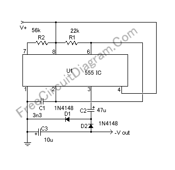
If a negative supply is required for an operational amplifier or if a negative bias voltage is needed while operating from a single supply voltage, such as in battery applications. To generate a negative supply voltage from a single positive...
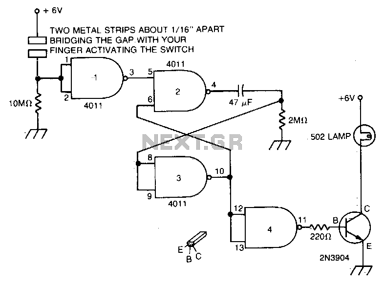
Touch the plate, and the light will turn on and remain on due to the 47 µF capacitor and the 2MΩ resistor for a duration determined by the timing resistor. The circuit described involves a touch-sensitive plate that activates a...
This post presents an interesting topic about switching power supply circuit diagrams for those who wish to learn more. A switching power supply is a type of power supply that uses a switching regulator to convert electrical power efficiently. Unlike...
Rosemary's original test circuit is shown in the article she tried to have published in a refereed scientific journal, but the submission was always rejected. In the last 5 months, I have had extensive email correspondence, and numerous telephone...
Infrared Remote Control Tester Circuit. This is a simple circuit that can be built to test infrared remote controls. The circuit utilizes an... This infrared remote control tester circuit is designed to verify the functionality of infrared remote controls commonly...
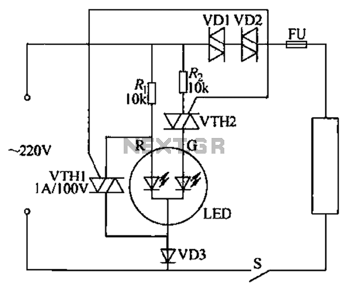
Color light-emitting diodes with different colors can indicate the operational status of electrical equipment, as illustrated in the accompanying figure. The red light-emitting diode (LED) R emits red light when energized, indicating that the 220V power supply is functioning...