
Seven kinds of analysis that sentence to the odd circuit implement method are compared
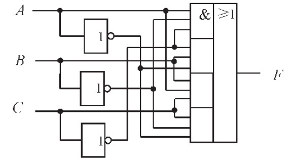
For the three input variables, designated as A, B, and C, the output function is represented by F. When an odd number of input variables are set to 1, the output function value is 1; conversely, when the number of 1s is even, the output function value is 0. A truth table for the odd circuit can be constructed based on this logical relationship. The three input odd circuit can be realized using inverters, AND gates, and OR gates. While this method does not alter the logical expression, it leads to a more complex circuit with increased wiring.
The three input variables can be processed through two different gate network design methods, both of which, despite their simplicity, result in excessive wiring and resource wastage. The logical function expression for the same logic problem does not have a unique representation. The third method utilizes XOR gates to implement the three input odd circuit, as illustrated in a referenced figure. The circuit depicted demonstrates that using XOR gates results in a simpler and clearer design compared to the previous methods, with fewer connections. Specifically, a single XOR gate can be used to realize the odd circuit by connecting two input variables, allowing for a more efficient circuit structure.
The decoder circuit structure, under suitable connection conditions, acts as a minterm generator. This capability enhances the understanding of combinational logic circuit design, providing a robust framework for analyzing and implementing various logical functions. The use of XOR gates not only simplifies the circuit but also optimizes resource utilization, which is a critical consideration in electronic design.The design of the combinational logic circuit is varied, I choose a kind of add even check circuit implementation to explain in detail. The parity check circuit has certain typicality and practicability in analysis and design of the combinational logic circuit, familiar with logic function and circuit implementation that is sentenced to the odd circuit,
contribute to strengthening the understanding of combinational logic circuit and mastering. Regard sentencing the example to the strange circuit implementation as, many kinds of ones that have discussed with gate network, Decoder, data selector have realized the scheme separately, demonstrate flexibility and diversity of circuit design of the combinatorial logic. As to the thing that the sentencing to the strange question of three input variables, set up its input variable and is indicated by A, B, C respectively, the output function is indicated by F.
When there is 1 of odd number one when made up in the value of the input variable, it is 1 to output function value; When the number of 1 is an even number in the value of the input variable is made up, it is 0 to output function value, can list and write out three input variables and sentence the truth table of the odd circuit to be shown in Table 1 according to this kind of logical relationship. Realize three input to sentence to the odd circuit with the inverter, AND-gate, or gate, it features basically there is not a change in the expression, it is simple and clear to realize the route, the shortcoming is to wire more, the circuit is complicated.
Realized three input variables are sentenced to the odd circuit and can be obtained by two kinds of above-mentioned different gate network design methods, though the first method and method two realize logic simply, is all wired too much, waste resources. The logical function expression of the same logic question does not possess uniqueness. Output function expression 1 of very logic question of inputting declaring to three variables Vary and is shown as follows: The method three: According to the above-mentioned expression 2 Obtain, three input variables sentence to the odd circuit and can also adopt the XOR-gate to realize, its circuit is shown as in Fig.
3. Can be seen by the circuit illustrated in Fig. 3, as to the logic question that three input variables sentence to very, when adopting the XOR-gate to realize, compare in the first method and method two, there are less lines in the circuit, the circuit is simple and clear, it is simple to realize. Namely a XOR-gate can input the negate AND gate to realize by 4 times 2, so three input can input the negate AND gate to realize to sentence to the odd circuit by 8 times 2, the circuit is shown as in Fig.
4. The circuit structure of the Decoder shows, under the appropriate connection condition, the Decoder is actually a minterm generator. According to the algebraic 🔗 External reference
Related Circuits
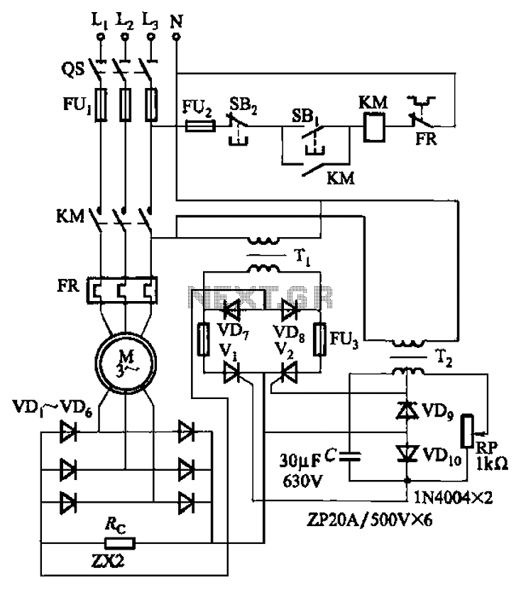
The circuit depicted in Figure 3-171 includes an auxiliary power supply that operates on single-phase AC power. It features a single-phase half-wave controlled bridge composed of diodes VD7, VD8, and thyristors V1, V2. The output current is managed by...

Connect the components, ensuring to pay attention to the connections for the transistor. The 22-ohm load resistor and thermistor should be connected in a manner that allows for good thermal contact. Note: If using the Light Application Adapter, REFIN-...

This is a simple circuit design for a two-station intercom system utilizing common 8-ohm mini speakers. The press-to-talk switches should feature a spring-return mechanism to ensure that the intercom cannot be left in the ON position. The circuit requires...

The 555 timer circuit, regardless of the manufacturer, has a consistent internal structure and performance. Various manufacturers produce different models of the 555 timer, including MC555, CA555, XR555, LM555, as well as domestic models like SL555, FX555, and 5G1555....
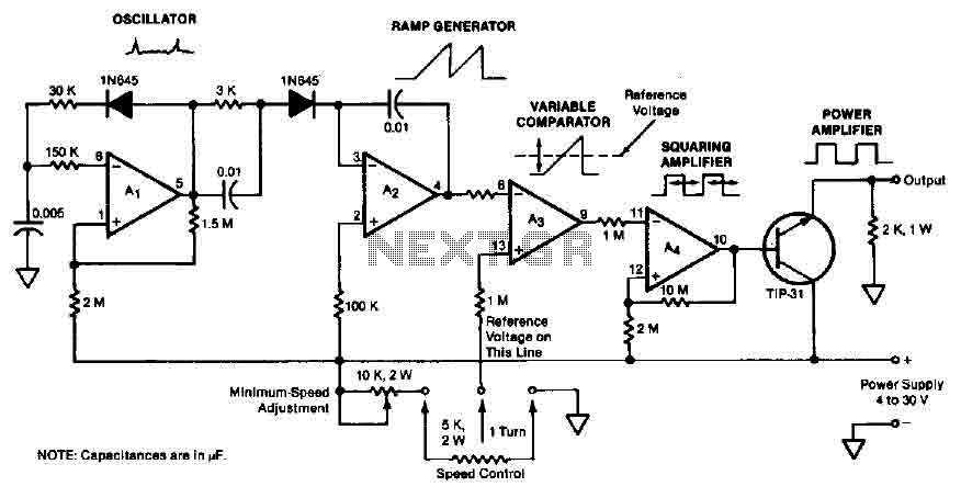
The quad operational amplifier circuit provides a pulse width modulation control ranging from 0 to 100 percent. The controller utilizes an LM3900 and operates with a single supply voltage between 4 to 30 V. A 1 kHz oscillator amplifier,...
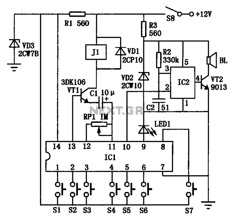
The automotive electronic locks circuit principle is illustrated with the dedicated lock IC 5G058. It features an external key switch connected to the positive power supply. The circuit includes six valid input keys, unlock keys S1 to S6, which...