
ac Validate Triac circuit
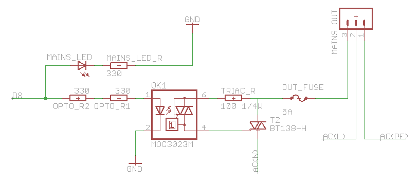
The thermal management of the triac in this circuit is critical, particularly considering the calculated thermal resistance of 10°C/W, which indicates that the triac could reach high temperatures under load. The calculation implies that, under maximum conditions, the device could operate at 110°C, which would greatly exceed typical operating limits for semiconductor devices. A heatsink with a lower thermal resistance is recommended to ensure reliable operation and to prevent thermal runaway.
The layout of the circuit on a two-layer board, with components spaced apart, is a consideration for both electrical performance and safety. The creepage distance of 6mm is a standard requirement for high-voltage applications, and the presence of a board between components may affect this distance. It is important to ensure that the design adheres to safety standards to minimize the risk of arcing or electrical failure.
Utilizing a MOSFET driven by D8 for controlling the photodiode is a prudent approach, as it allows for better current handling capabilities than a GPIO pin. The recommendation to exceed the minimum current specification of 5mA is essential for ensuring reliable operation of the photodiode.
In terms of circuit protection, the inclusion of fuses in both the live and neutral lines is a best practice to enhance safety. This prevents potential hazards associated with having only the neutral line fused, which could leave the circuit energized and pose risks of electric shock.
For the inductive nature of the heater load, implementing the resistor-capacitor-resistor gate scheme will help to mitigate false triggering of the triac due to voltage spikes or noise. This design consideration will improve the stability and performance of the circuit.
Overall, careful attention to thermal management, component layout, current handling, and circuit protection will ensure the reliability and safety of the triac-based control circuit for the heater load.The heatsink on the triac is a bit unclear for me. I`ve calculated a maximum value of 10C/W, is this fine My calculation is: (max temp - room temp)/(max on stage voltage * (milli amps / voltage) - junction to base themal resistance (110-25)/(1. 65*(1000/230)-1. 5 = ~10. 35). Does this mean the triac will be at 110c all the time, seems a bit high to me. Ideally i would have a smaller heatsink though so i hope this is wrong :) Most of this circuit is on the bottom of a 2 layer 1. 6mm board with other components min 4mm away on the top. From what i understand the creepage distance should be min 6mm but is it the same with the board in between It`s probably safer to have D8 drive a small MOSFET to control the photodiode instead of relying on the current-sourcing capability of the GPIO pin itself.
You should also provide a bit more than the absolute minimum 5mA cited by the datasheet. A fuse should always be in the line - never only in the neutral. (Fusing both is OK. ) If you fuse only the neutral, you still have a path from line to earth since in most jurisdictions, neutral is earthed somewhere. Dangerous and potentially lethal. Your heater load is most likely inductive in nature, so you should consider the resistor-capacitor-resistor gate scheme shown on page 6 of the datasheet to desensitize the gate.
You can always no-populate the capacitor later if you don`t need it. The device (without heatsink) has a junction-to-ambient resistance of 60K / W. Since your 1000W heater would draw around 4. 34A of current when the triac is conducting, at 230VAC that`s ~7W - at 100VAC it`s more like 16. 5A. You`ll definitely need a heat sink :) 🔗 External reference
Related Circuits
Previously, a boost circuit was tested that enables the powering of a 3 V LED using a discharged battery (approximately 1 V or lower). This circuit consists of a single transistor, one resistor, and a small transformer with a...

A quad op-amp serves as the core component of this function generator. U1A produces a square wave, which is outputted to J8. J1 and J2 are pulse outputs derived from differentiating the square wave. The integrator U1B creates a...
Color sensing using a camera and a sufficiently powered processor that runs image histogram logic (or similar algorithms) can reliably determine the presence of specific colors. However, alternatives that are significantly more cost-effective for detecting the presence or absence...
Continuity tester to check continuity in the circuit (Insakittochekka) is. The continuity check over the circuit board wiring that can be checked at a lower voltage semiconductors do not conduct contained in the circuit, you can just check the...
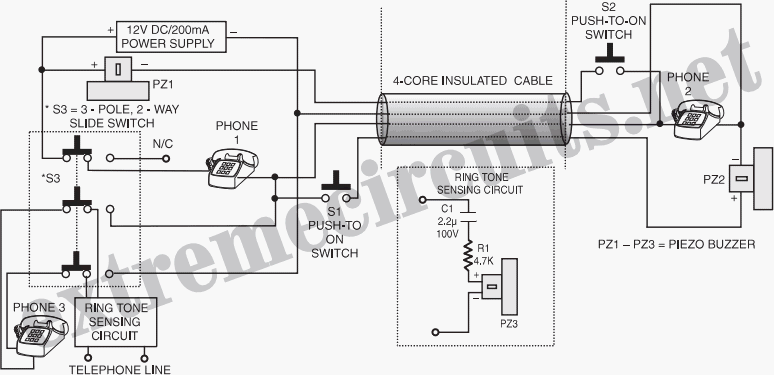
The circuit described can connect two telephones in parallel and function as a two-line intercom. Typically, a single telephone is connected to a telephone line. When another telephone is needed at a distance, a parallel line is utilized for...
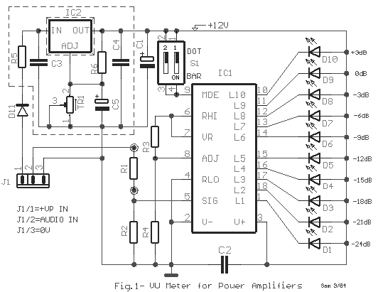
This is an upgraded circuit based on the Simple Volume Unit Display Circuit Diagram 1, featuring enhanced power for the audio input. Components include resistors. The upgraded circuit enhances the functionality of the original Simple Volume Unit Display by incorporating...
Warning: include(partials/cookie-banner.php): Failed to open stream: Permission denied in /var/www/html/nextgr/view-circuit.php on line 713
Warning: include(): Failed opening 'partials/cookie-banner.php' for inclusion (include_path='.:/usr/share/php') in /var/www/html/nextgr/view-circuit.php on line 713