
ADUC831 1.3MIPS 8052 MCU + 62kB Flash + 8-Ch 12-Bit ADC + Dual 12-Bit DAC

The ADUC832 MicroConverter is designed to facilitate a wide range of applications, particularly in the fields of industrial automation, medical instrumentation, and sensor interfacing. Its integration of high-performance analog and digital components on a single chip significantly reduces the complexity and size of electronic systems. The 12-bit ADC allows for precise measurement of analog signals, while the dual DACs enable the generation of accurate analog outputs for control applications.
The microcontroller core, based on the 8052 architecture, supports a variety of programming environments and development tools, making it accessible for developers familiar with the 8051 instruction set. The extensive memory resources, including both program and data memory, ensure that complex algorithms and data processing tasks can be executed efficiently.
The programmable clock divider is a critical feature, allowing for flexible adjustment of the MCU clock frequency to meet specific application requirements. This adaptability, combined with the integrated communication interfaces (SPI, I2C, and UART), facilitates seamless integration into existing systems and enhances connectivity with other devices.
The ADUC832's built-in watchdog timer and various timer counters provide essential functionality for real-time applications, ensuring system reliability and facilitating time-based operations. The presence of a power supply monitor and bandgap reference further enhances the device's robustness, enabling it to operate reliably across varying conditions.
Overall, the ADUC832 MicroConverter represents a versatile solution for modern electronic design, offering a compact and efficient platform for data acquisition and control tasks.The ADUC832 MicroConverter is a fully integrated 12-bit data acquisition system-on-a-chip. Like all of ADI`s MicroConverter products, it features precision A/D & D/A conversion and a Flash Microcontroller on a single chip. The ADUC832 is 100% hardware backward compatible with the ADUC812 except that it requires a different crystal.
If you require full hardware backward compatibility with the ADUC812 use the ADUC831 instead. The ADUC832 is available in 52-pin PQFP or 56-pin CSP packages and operates on a 3V or 5V power supply. The ADUC832 is a complete smart transducer front end, integrat- ing a high performance self-calibrating multichannel 12-bit ADC dual 12-bit DACs and programmable 8-bit MCU on a single chip.
The device operates from a 32 kHz crystal with an on-chip PLL generating a high frequency Clock of 16. 77 MHz. This Clock is, in turn, routed through a programmable Clock divider from which the MCU core Clock operating frequency is generated.
The micro- controller core is an 8052 and therefore 8051 instruction set compatible with 12 core Clock periods per machine cycle. 62 kBytes of nonvolatile Flash EE program memory are provided on-chip. 4 kBytes of nonvolatile Flash EE data memory, 256 bytes RAM, and 2 kBytes of extended RAM are also integrated on-chip.
The ADUC832 also incorporates additional Analog functionality with two 12-bit DACs power supply monitor, and a band gap reference. On-chip digital peripherals include two 16-bit - DACs dual output 16-bit PWM, watchdog Timer time interval Counter three Timers Counters Timer 3 for baud rate generation, 2 and serial I/O ports (SPI, I C, and UART) By Analog Devices, Inc.
🔗 External reference
Related Circuits

In conventional triangular-wave oscillators, hysteresis from positive feedback in the Schmitt trigger determines the voltage levels and amplitude of the triangular waves. With this topology, it is difficult to independently vary the voltage levels and amplitude of the output...
All of the components in this list are generally available through RadioShack for less than $20. It is highly recommended to use a breadboard for assembly, as mistakes are common for first-time builders, and soldering can complicate troubleshooting. This...
The following article is a continuation of the application note titled "Defining and Testing Dynamic Parameters in High-Speed ADCs, Part 1." It outlines the test conditions and setup recommendations necessary for effectively measuring the dynamic performance parameters of high-speed...
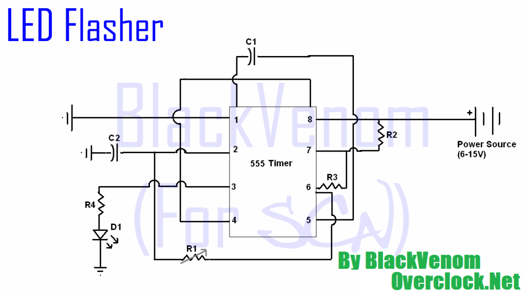
This is a compact LED flasher circuit designed using the 555 timer integrated circuit (IC), powered by two 1.5V batteries. The circuit can function as a flashing metronome, dark room timer, reminder, or for other similar applications. In the...
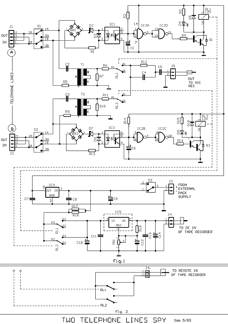
Many times exists the need recording some conversations from a telephone line and this it's relatively easy. If we want however to have the possibility recording from two telephone lines simultaneously in a tape recorder, we needed a circuit...
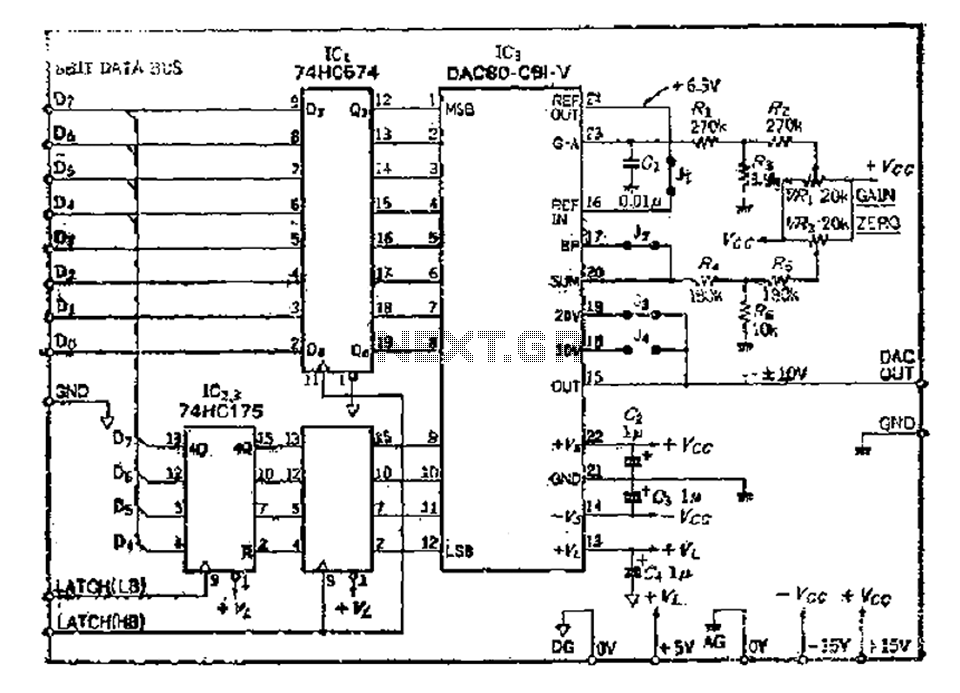
The 8 microcomputer data operates with an 8-bit parallel output, while also accommodating serial input for D-A converters. Typically, data must be entered in two groups and processed as a whole. The requirements for data latching involve 16 straight...