
ADUC836 1MIPS 8052 MCU + 62kB Flash + Dual 16-Bit ADC + 12-Bit DAC

The ADUC841, ADUC842, and ADUC843 are highly integrated devices designed for smart transducer applications, combining various functionalities into a single chip to enhance efficiency and reduce design complexity. The multichannel ADC is capable of self-calibration, ensuring accurate data conversion from analog to digital signals, which is critical in sensor applications. The dual DAC allows for precise analog signal generation, making these devices suitable for applications that require both sensing and control.
The clocking mechanism of the ADUC841 and ADUC842 is a key differentiator. The ADUC841's direct connection to an external crystal oscillator allows for flexibility in clock frequency selection, accommodating a range of applications that may require higher processing speeds. In contrast, the ADUC842's use of a 32 kHz crystal with an on-chip PLL provides a more stable clock source with programmable capabilities, making it ideal for lower-power applications that still demand reasonable performance.
The absence of analog DAC outputs in the ADUC843 suggests its intended use in applications where digital processing and control are prioritized over analog signal generation. This variant may be particularly useful in systems where the DAC functionality is not required or is handled externally.
The integrated 8052 core microcontroller enhances the overall performance of these devices, providing a powerful processing unit capable of executing instructions at a peak performance of 20 MIPS. This efficiency is crucial for real-time processing in transducer applications, where rapid response to changing conditions is necessary.
Memory options available with these devices further augment their versatility. The substantial non-volatile Flash EE program memory allows for the storage of complex algorithms and firmware, while the data memory supports data logging and other memory-intensive tasks. The combination of RAM and extended RAM provides additional flexibility for temporary data storage during processing, making these devices suitable for a wide range of embedded applications.
Overall, the ADUC841, ADUC842, and ADUC843 represent a robust solution for developers seeking to implement smart transducer technology in their designs, offering a rich set of features in a compact form factor.The ADUC841 ADUC842 ADUC843 are complete smart transducer front ends, that integrates a high performance self- calibrating multichannel ADC a dual DAC and an optimized single-cycle 20 MHz 8-bit MCU (8051 instruction set compatible) on a single chip. The ADUC841 and ADUC842 are identical with the exception of the Clock Oscillator circuit; the ADUC8 41 is clocked directly from an external crystal up to 20 MHz whereas the ADUC842 uses a 32 kHz crystal with an on-chip PLL generating a programmable core Clock up to 16. 78 MHz. The ADUC843 is identical to the ADUC842 except that the ADUC843 has no Analog DAC outputs. The Microcontroller is an optimized 8052 core offering up to 20 MIPS peak performance. Three different memory options are available offering up to 62 kBytes of nonvolatile Flash EE program memory.
Four kBytes of nonvolatile Flash EE data memory, 256 bytes RAM, and 2 kBytes of extended RAM are also integrated on-chip. By Analog Devices, Inc. 🔗 External reference
Related Circuits
DAC stands for Digital to Analog Converter. This article explores the code created by Michael Smith for a PWM-based DAC. The code has been modified to allow for the testing of various DAC options. A comparison is made between...
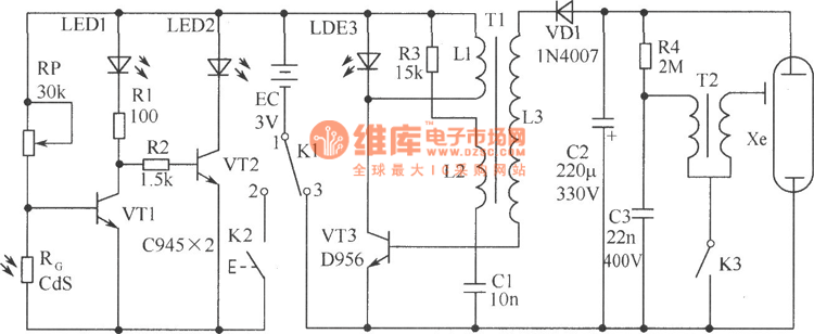
The circuit consists of a light metering circuit and a flash circuit, as illustrated in the accompanying image. It is designed for use with integrated cameras such as POPTICS, Franka X-500, and WIZEN-860S. The circuit includes the following components:...
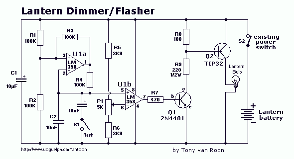
The electronic lantern control circuit adds high-efficiency dimming and flashing to an existing battery-powered lantern or flashlight or to a custom design. For the car it makes a great lamp for changing a flat tire, back seat reading or...
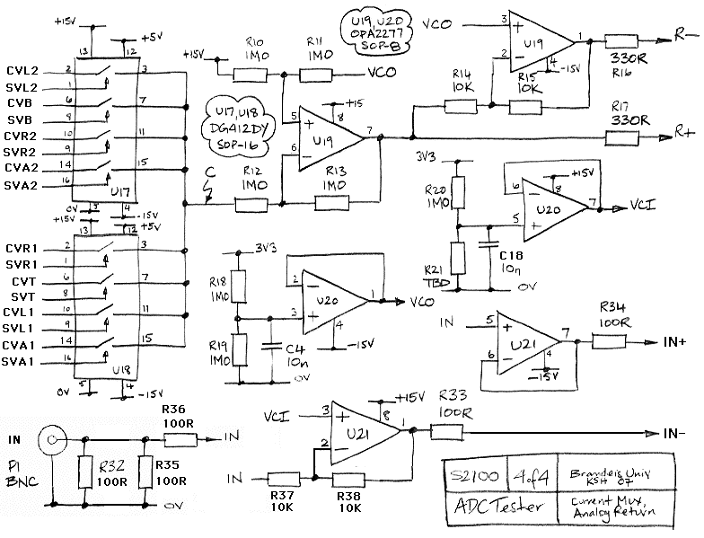
The ADC Tester (A2100) is a LWDAQ device that records the output and power consumption of two ADCs. Its original purpose was comparative testing of two ADCs at different temperatures, but it has also proven to be an effective...
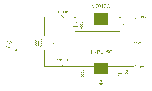
In this circuit, the 7815 regulates the positive supply, and the 7915 regulates the negative supply. The transformer should have a primary rating of 240/220 volts for Europe, or 120 volts for North America. The centre tapped secondary coil...
This circuit sequentially lights ten bulbs, first in one direction and then in the opposite direction, creating an appealing visual effect. Gates N1 and N2 form an oscillator, which serves as a clock for the BCD up/down counter CD4510...