
AM balanced diode circuit
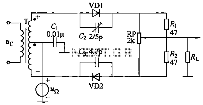
The common diode balanced modulator circuit is an essential component in communication systems, particularly for amplitude modulation (AM) applications. The circuit's design utilizes two identical diodes, which ensures that the modulation process is symmetrical and efficient. The center-tapped transformer plays a crucial role in the circuit by providing the necessary phase shift and balancing the input signals.
In this configuration, the low-frequency modulation signal is applied to one side of the transformer, while the high-frequency carrier signal is applied to the other side. The diodes, VD1 and VD2, are configured to allow current flow in only one direction, effectively mixing the two signals. This results in the generation of upper and lower sidebands, which are characteristic of amplitude modulation.
The 2AP9 diodes are chosen for their reliable performance in radio frequency applications, ensuring that the circuit can handle the required power levels without distortion. The circuit's simplicity is an advantage, as it requires fewer components compared to other modulation techniques, leading to reduced costs and improved reliability.
The output of the balanced modulator is a high-amplitude modulated signal, which can then be further processed or transmitted. The minimal harmonic output is particularly beneficial in reducing interference and improving the overall quality of the transmitted signal. The circuit's design is adaptable, allowing for adjustments in the transformer turns ratio or diode biasing to optimize performance for specific applications. Overall, this balanced modulator circuit is a fundamental building block in the field of amplitude modulation, widely utilized for its effectiveness and efficiency in signal processing. Common diode balanced modulator circuit is shown. It consists of two identical performance diodes and a center-tapped transformer T composition. Diodes VD1, VD2 are 2AP9. Other elements parameters Parameter test value as shown in FIG. 21-37. Diode function is to balance the amplitude modulation circuit low-frequency modulation signal and high-frequency carrier signal through the circuit into a high-amplitude modulated signal output. The amplitude modulation circuit is simple structure, less harmonic output, is a common amplitude modulation circuit.
Related Circuits
This is a light sensor circuit designed to detect darkness, utilizing the op-amp 741 integrated circuit as the primary control element. The circuit is straightforward and specifically designed to sense light during nighttime. The light detection is accomplished using...
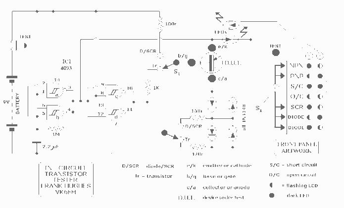
The design shown will test PNP and NPN transistors, diodes and SCRs both "in-situ" (equipment of course de-energised) and also by direct connection to a stand-alone component. It is a simple GO/NOGO test which can identify diode and transistor...
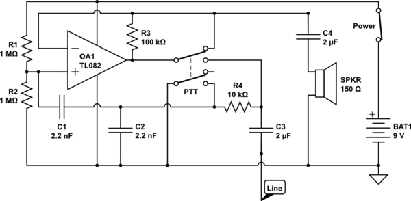
The circuit operates in receive mode, with the Push-To-Talk (PTT) switch enabling transmit mode. The speaker functions as both a microphone and a speaker. Most systems observed utilize a rocking armature transducer for the speaker. There is no base...
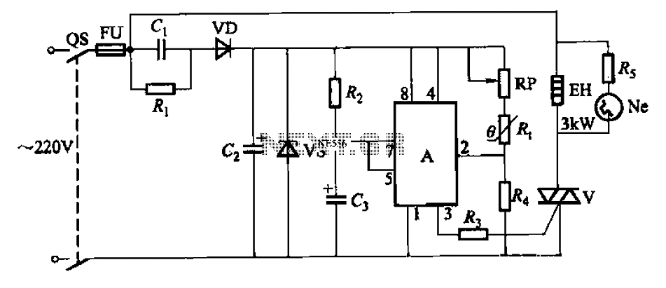
An automatic temperature control circuit is designed for climate control thermostats. Its primary function is to maintain a constant internal temperature using an electric heater (EH). The control mechanism utilizes a negative temperature coefficient thermistor as the temperature sensing...

This circuit is designed to charge between one and twelve NiCd cells using a car battery. With switch S1 set to the normal position, it is capable of charging up to six cells. The circuit operates by utilizing a car...
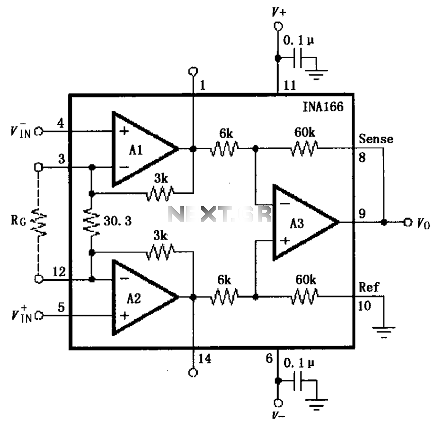
The basic connection circuit for the INA166 includes signal and power connections. A 0.1 µF tantalum capacitor should be used for filtering the chip's power supply terminal, and the PCB layout should be designed to position this capacitor as...