
Transistor and diode tester
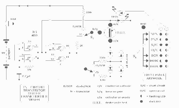
The circuit operates as a versatile semiconductor tester capable of evaluating PNP and NPN transistors, diodes, and silicon-controlled rectifiers (SCRs) in both in-circuit and out-of-circuit configurations. The core of the design utilizes a CD4093 CMOS integrated circuit configured as a square-wave oscillator, generating a frequency of approximately 2 Hz. This oscillator output is then inverted by additional gates within the same IC, producing complementary square wave signals that serve as the testing voltage for the device under test (D.U.T.).
The biasing of the transistor's base is achieved through a 1000-ohm resistor, ensuring proper operation during testing. Red LEDs are employed in a unique configuration, arranged in a "contra" fashion across the output. This arrangement allows for visual indication of the D.U.T.'s status, with current flow through the LEDs being limited by a 470-ohm resistor. The design cleverly utilizes the forward voltage drop characteristics of the LEDs, clamping the peak inverse voltage (P.I.V.) to approximately 1.7 volts, which corresponds to the ON-state voltage of the conducting LED.
When the TEST button is engaged without a D.U.T. connected, both LEDs will alternately flash, indicating the circuit's functional status. Upon connecting a healthy transistor, the testing mechanism operates such that during the half-cycle when the transistor is biased ON, one LED will darken as it becomes effectively short-circuited, while the other LED will illuminate during the off half-cycle, resulting in a visible 2 Hz flashing pattern.
The functionality of the circuit is further enhanced by the inclusion of series-connected silicon diodes, which serve to ensure that current only flows through the D.U.T. when it is fully saturated. This design avoids the need for desoldering components, thereby streamlining the testing process. The switch S1 allows for the selection between testing configurations for diodes and SCRs, facilitating the removal of one diode from the series connection to accommodate the forward voltage drop of the D.U.T. This ensures accurate readings without interference from the additional voltage drops present in the circuit.
Overall, this circuit design exemplifies an efficient and practical approach to semiconductor testing, providing clear visual feedback and minimizing the need for manual intervention.The design shown will test PNP and NPN transistors, diodes and SCRs both "in-situ" (equipment of course de-energised) and also by direct connection to a stand-alone component. It is a simple GO/NOGO test which can identify diode and transistor action and will indicate diode polarity and transistor type PNP/NPN, if this is unknown.
The CD4093 CMOS IC (IC1a & b) is configured as a square-wave oscillator of about 2Hz. IC1 c & d invert this 2Hz signal. These two complementary square wave voltages are used as the test supply voltage to the Device Under Test (D.U.T.). Transistor base bias is via a 1000-Ohm resistor. Two red LEDs are paralleled in ?contra? fashion and connected across the output. Current flow through either led is limited by the 470 Ohm resistor and either LED?s P.I.V. is clamped to about 1.7v, which is the ON-state voltage of the other LED (being in the conducting state). With no D.U.T. connected to the tester, and TEST push button pressed, both LEDs will flash alternately. If a healthy transistor is now connected: during the half-cycle during which it will be biased ON and therefore heavily conducting, one LED will be effectively short-circuited and remain dark.
On the alternate half-cycle, the polarity of the applied signal will not cause the D.U.T. To switch ON and current can then flow through one led causing it to illuminate. This appears as a 2Hz flashing of the LED. It should therefore be evident that if the D.U.T. is: 1. Shorted; both LEDs will be dark and 2. Open Cct; both LEDs will flash. The purpose of the two strings of series connected silicon diodes, connected in series with the D.U.T. may require some explanation: Their function is to allow only a current pathway through the D.U.T. provided that it is in fact fully saturated (turned hard-ON) and that insufficient current could flow through parallel circuit resistances such that one or both of the LEDs would be dark due to this.
Remember this design is called an "in-circuit" tester (no messy de-soldering, to isolate a suspect faulty semiconductor!). In order to test SCRs and diodes, S1 is thrown to the appropriate position, in which one of each of the two series connected pair of diodes is switched out.
This is necessary because: the forward ON-state voltage of a healthy diode or SCR being about 0.7 volt, then three conducting series junctions would present about 2.1 Volt across the LED, which should normally be dark. If you have any questions related to this project then please refer them to the author Frank V. Hughes 🔗 External reference
Related Circuits
Rsense will cause Q2 to conduct when a threshold of approximately 0.65V is reached. Rbias will determine the extent of this limitation, although this aspect remains unclear. Particularly, if Rsense is positioned on the high side, simply activating Q2...

With this tester you can check whether a diode is working properly. In the table you can see what LED to indicate the positions of the switch and condition of the diode. The circuit can be connected to a...
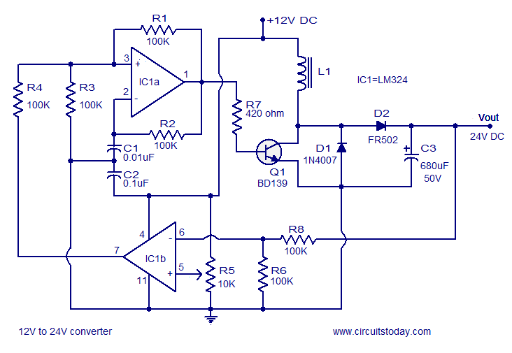
A simple 12V to 24V DC-DC converter circuit diagram built around the LM324. This boost converter schematic can provide up to 800mA output current and a steady 24V DC. The described circuit utilizes the LM324 operational amplifier as the core...

This circuit consists of three single-junction transistor time relay circuits utilizing a pulse charging mechanism, allowing for extended delay times of up to several minutes. The first stage delay circuit incorporates unijunction transistors (VTi) and other components, where capacitor...
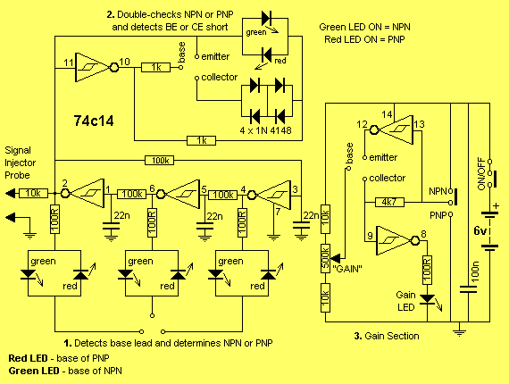
There have been a lot of transistor tester circuits in recent electronics magazines, but this one is different. It has more features and includes a signal injector so you can test audio sections of radios and the front end...

Bipolar transistor amplifiers must be properly biased to operate correctly. In circuits made with individual devices (discrete circuits), biasing networks consisting of resistors are commonly employed. More elaborate biasing arrangements are used in integrated circuits, such as bandgap voltage...
Warning: include(partials/cookie-banner.php): Failed to open stream: Permission denied in /var/www/html/nextgr/view-circuit.php on line 713
Warning: include(): Failed opening 'partials/cookie-banner.php' for inclusion (include_path='.:/usr/share/php') in /var/www/html/nextgr/view-circuit.php on line 713