
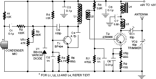
am transmitter circuit
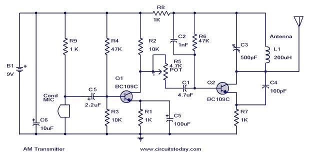
The AM transmitter circuit operates by converting audio signals into radio frequency signals suitable for transmission. The audio amplifier section amplifies the microphone's audio output before it enters the oscillator stage. The oscillator, which is pivotal in generating the RF carrier wave, utilizes the BC109 transistor (Q1) in conjunction with the tank circuit formed by L1 and VC1. This tank circuit is critical for determining the frequency of the transmitted signal, allowing for tunability within the specified range.
The regenerative feedback mechanism enhances the oscillation stability and amplitude. By connecting the base and collector of Q1 across the tank circuit, the circuit ensures that the oscillation builds up effectively. The coupling capacitors (C2 and C4) are essential for transferring signals between stages while blocking DC components, which could interfere with performance.
The common emitter configuration of Q2 allows for significant amplification of the RF signal, making it suitable for transmission. The decoupling capacitor (C5) ensures that the gain is maximized by isolating the emitter from any loading effects, which could otherwise reduce the amplification.
The microphone input is critical for capturing audio, and the choice of an electret condenser microphone is appropriate due to its sensitivity and ease of use. The variable resistor (R5) allows for fine-tuning of the modulation depth, providing flexibility in adjusting the transmitter's output according to the user's requirements.
Overall, this AM transmitter circuit serves as a practical solution for personal audio transmission, adhering to regulatory standards while delivering satisfactory performance for localized broadcasting.Here is the circuit diagram of a simple AM transmitter circuit that can transmit your audios to your backyard. This circuit is designed with limited power output to match the FCC regulations and still produces enough amplitude modulation of voice in the medium wave band to satisfy your personal needs.
You will love this!. The circuit has two parts, an audio amplifier and a radio frequency oscillator. The oscillator is built around Q1 (BC109) and related components. The tank circuit with inductance L1 and capacitance VC1 is tunable in the range of 500kHz to 1600KHz. These components can be easily obtained from your old medium wave radio. Q1 is provided with regenerative feedback by connecting the base and collector of Q1 to opposite ends of the tank circuit.
C2, the 1nF capacitance, couples signals from the base to the top of L1, and C4 the 100pF capacitance ensures that the oscillation is transfered from collector, to the emitter, and through the internal base emitter resistance of the transistor Q2 (BC 109), back to the base again. The resistor R7 has a vital part in this circuit. It ensures that the oscillation will not be shunted to ground trough the very low value internal emitter resistance, re of Q1(BC 109), and also increases the input impedance such that the modulation signal will not be shunted to ground.
Q2 is wired as a common emitter RF amplifier, C5 decouples the emitter resistance and unleashes full gain of this stage. The microphone can be electret condenser microphone and the amount of AM modulation can be adjusted by the 4.
7 K variable resistanceR5. 🔗 External reference
Related Circuits
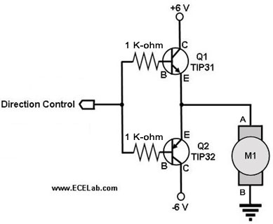
The following circuit illustrates a two-transistor DC motor driver circuit diagram. This circuit utilizes the TIP32 transistor. Features: operates in... The two-transistor DC motor driver circuit is designed to control the operation of a DC motor using two NPN transistors,...
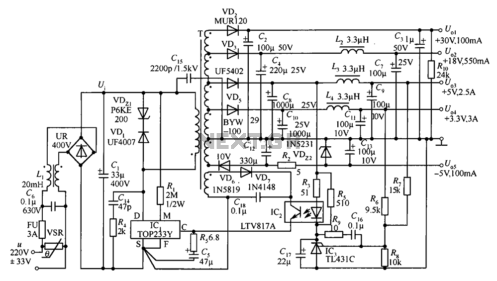
A 35W switching power supply circuit designed for a set-top box output is depicted in Figure 5. It features five distinct voltage outputs: Uo1 (+30V, 100mA), Uo2 (+18V, 550mA), Uo3 (+5V, 2.5A), Uo4 (+3.3V, 3A), and Uo5 (-5V, 100mA)....
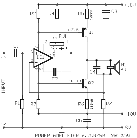
The amplifier circuit utilizes negative current feedback, which ensures that the load current is primarily influenced by the input signal rather than the loudspeaker's impedance. The inductor current from the loudspeaker generates a voltage across resistor R7, which is...
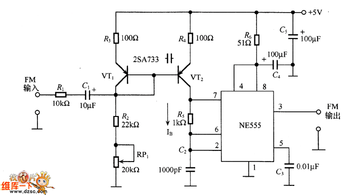
The figure illustrates an NE555 frequency modulation (FM) circuit. In this circuit, pin 7 of the NE555 is connected to an FM modulation section that consists of resistor R5 and capacitor C2, although the frequency range is somewhat limited....
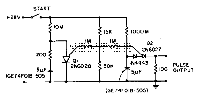
The circuit reduces the effective peak current of the output PUT, Q2. It allows the capacitor to charge with a high gate voltage and periodically lowers the gate voltage. When Q1 fires, the timing resistor can be set to...
The wireless transmitter circuit utilizes transistor T1 (BF494) as a low-power variable-frequency VHF oscillator. A varicap diode circuit is incorporated to modify the frequency of the FM transmitter and to facilitate frequency modulation using audio signals. The output power...