
AMPLITUDE MODULATOR 1
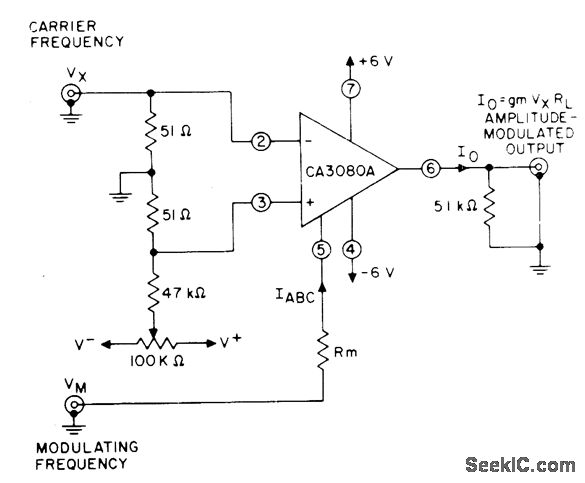
The described circuit employs the CA3080A, a versatile operational amplifier known for its ability to handle various signal processing tasks. The operational amplifier is configured in a way that allows for dynamic adjustment of its gain based on the bias current, IABC. By manipulating this bias current, the circuit can achieve precise control over the amplification of input signals.
The modulating voltage (Vm) plays a crucial role in this configuration. As Vm varies, it influences the amount of current flowing through the resistor Rm. This change in current directly affects the biasing of the operational amplifier, thereby modulating the gain applied to the carrier signal. The result is an amplitude modulation effect, where the output signal's amplitude reflects the variations in the modulating voltage.
The circuit's design highlights the importance of feedback and stability in operational amplifier applications. Proper selection of resistor values and careful consideration of the power supply are essential to ensure optimal performance. The CA3080A's characteristics, such as its low distortion and wide bandwidth, make it suitable for applications requiring high-fidelity signal processing.
In summary, this circuit effectively demonstrates the principles of gain control and amplitude modulation using a variable operational amplifier, showcasing its utility in various electronic communication and signal processing applications. Proper implementation can lead to enhanced signal integrity and improved performance in systems relying on amplitude modulation techniques.Uses controlled variation of amplifier bias current IABC in CA3080A variable opamp to obtain effective gain control of signal. Variations in amplitude of modulating voltage Vm change bias current through Rm to give amplitude modulation of carrier.
-"Circuit Ideas for RCA Linear ICs, " RCA Solid State Division, Somerville, NJ, 1977, p 15. 🔗 External reference
Related Circuits
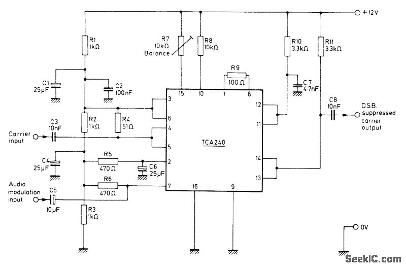
The Mullard TCA240 is a dual balanced modulator-demodulator that effectively suppresses the carrier frequency at the output, which is essential for Single Sideband (SSB) or Double Sideband (DSB) operation in transmitters. The bias resistor R7 is adjustable to achieve...
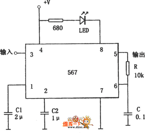
The figure illustrates the 567 FM demodulator circuit. The FM signal is received at pin 3, while the demodulated output signal is available at pin 5. The central frequency of the FM signal that the circuit can demodulate is...

Two integrated circuit (IC) RF modulators are utilized to convert a suitable baseband video and audio signal into a low VHF modulated carrier, specifically channels 2 through 6 in the U.S. and channels 1 through 3 in Japan. The...
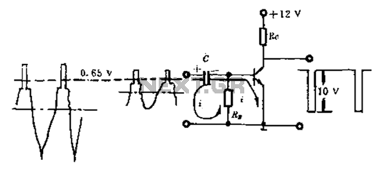
Amplitude separation circuit. A typical amplitude separating circuit is composed of a transistor, capacitance C, and resistances RB and RC. The input signal is a composite video signal, typically with a peak-to-peak voltage of about 2V. The output signal...
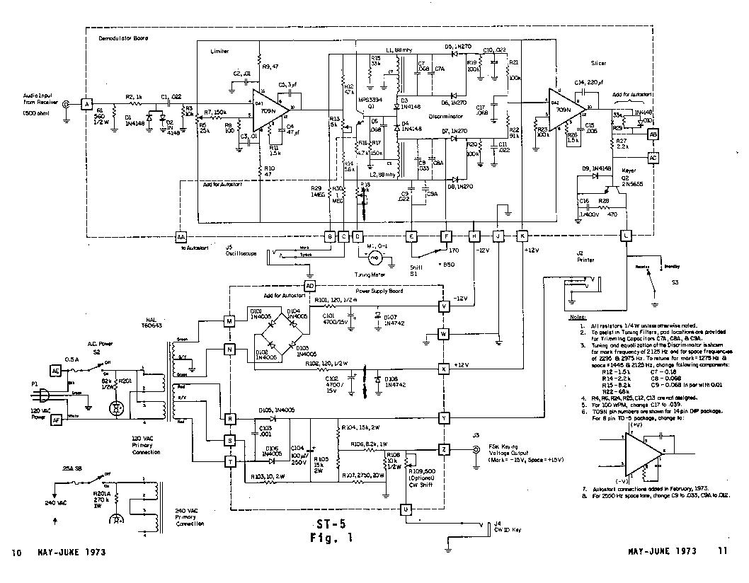
The Mainline ST-5 was introduced in the RTTY Journal in May 1970 and has quickly become a popular demodulator for RTTY. Due to the unavailability of back issues, the original article is being reprinted. Those interested in 100 baud...
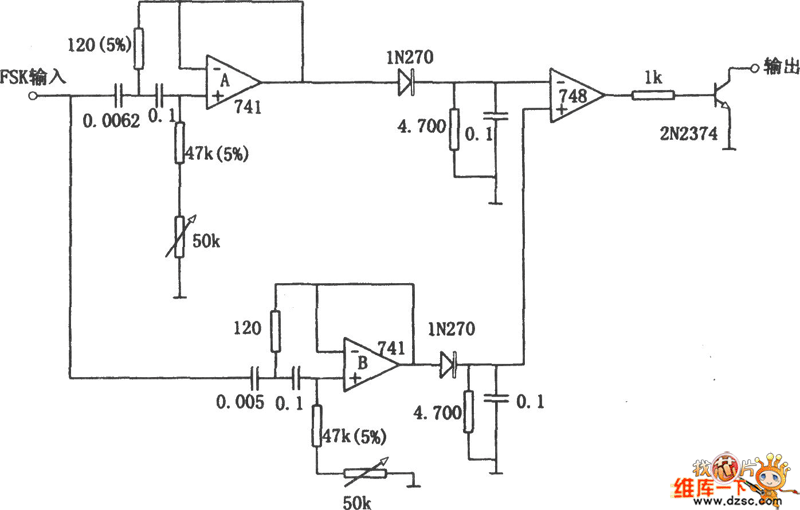
Replacing the LC modulation circuit with an active filter allows for the elimination of large and costly inductance coils in frequency shift key control demodulators. This approach not only reduces the size of the circuit but also enhances the...