
Amplitude separation circuit diagram
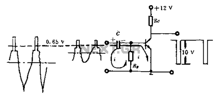
The operation of the amplitude separation circuit is as follows: without a DC bias, the transistor remains off when there is no signal, resulting in no voltage drop across RC and an output power level of +12V. Upon receiving the composite video signal, the emitter junction capacitance C and resistance RB form a detection circuit. When the signal voltage exceeds 0.65V during the synchronization pulse, the emitter becomes active, charging capacitor C. After the sync pulse, when the signal voltage drops below 0.65V, the emitter junction ceases conduction, and the charge on capacitor C discharges through RB and the signal source, as indicated in the circuit. If the signal waveform repeats over multiple line periods, the charging and discharging stabilize, and the voltage across capacitor C reflects the average signal voltage, effectively filtering out the DC component.
The transistor conducts only during the sync pulse, resulting in a negative pulse at the output across RC, with a pulse width determined by the power supply voltage minus the transistor's saturation voltage, exceeding 10V. This process effectively extracts the sync pulse from the composite video signal. Additionally, the circuit provides clamping action, ensuring the sync tip level remains clamped at 0.65V. The emitter junction functions as a clamping diode.
The necessity for clamping arises from variations in the average image signal level, which can shift the sync tip due to changes in screen brightness or signal intensity caused by factors such as location, antenna orientation, and surrounding structures. Despite the presence of an automatic gain control (AGC) circuit, the output level can still experience significant fluctuations. Therefore, a fixed level for synchronization cutting is inadequate, as it may misalign with changes in signal amplitude and mean, leading to synchronization instability and visual artifacts.
The characteristics of the circuit ensure that when the input signal amplitude varies, the average voltage on capacitor C adjusts accordingly, maintaining the base voltage at 0.65V, which fluctuates with the signal amplitude. The transistor operates in an off state most of the time, activating only during the sync pulse. To achieve a reliable output pulse waveform, the transistor must switch effectively, with a low saturation voltage to guarantee a 10V output amplitude. The value of capacitor C must be carefully selected; it should not be too small to prevent inadequate charging time constants that could affect the sync tip, nor too large to hinder the circuit's ability to respond quickly to changes in image content. Typically, capacitor values range around 1µF.
The input signal is negative, while the output signal from the detector circuit is predominantly positive. The amplitude of the positive polarity composite video signal is processed by the separation circuit, which utilizes a PNP type transistor. The transistor activates during the synchronization header and remains off otherwise. An output resistor is connected between the collector and ground to produce the output pulse, which maintains an amplitude above 10V. Bias resistors of 68kΩ and 510kΩ provide a slight bias to the base of the transistor, enhancing synchronization sensitivity.Amplitude separation circuit A typical amplitude separating circuit shown in Figure 1. It is composed of a transistor and a capacitance C, resistance RB, RC constituted. After detecting the input signal is a video composite video signal, usually peak to peak at about 2V. The output signal is a composite sync signal, for simplicity, the figure only depicts the horizontal synchronizing pulse, in the circuit of Figure 1, it is down, the range of 10V or more. Amplitude separation circuit works: Transistor without a DC bias, when there is no signal it is off, no voltage drop on the RC, the output of the power level of + 12V.
When the video composite video signal arrives, the transistor emitter junction capacitance C, resistance RB constitute a similar detection circuit, the signal voltage is greater than 0.65V internal synchronization pulse time, the emitter is turned on, the capacitor C is charged, the charging current i charging path as shown in Fig. When the sync pulse in the past, the signal voltage is lower than 0.65V, the emitter junction is not conducting, the charge on the capacitor C through RB and the signal source (front stage) discharge, i put the path shown.
If the signal waveform is repeated a plurality of line periods, the charging, discharging down stable equilibrium, the voltage on the capacitor C is equal to the average value of the signal voltage. In other words, the capacitor C voltage signal DC component (average value) cut off. Transistor only during the sync pulse conduction time, a voltage drop, the output voltage on RC becomes negative pulse shown in Fig., A pulse width of the power supply voltage minus the tube saturation voltage greater than 10V.
This completes the sync pulse cut from the composite video signal is applied to the video. Also has a clamping action in the circuit of Figure 1, it makes the sync tip level is always up and down clamp 0.65V. Emitter junction plays a clamping diode. Necessity clamp: the average value of the image signal with the image content to be changed when the screen is dark, the average level moves upward, approaching the black level.
Conversely, when the screen appears bright scenes, the average level down will tend white level. In addition, the intensity of the received signal due to factors of location, antenna orientation and distribution of the surrounding buildings and so on have a greater change, although the receiver using an automatic gain control (AGC) circuit, but the output level will have put percent changes over tens. So after the video detection Queensland composite video signal whose amplitude is still some changes, so should not adopt a fixed level to synchronize the cutting head, otherwise, when the signal amplitude and mean changes in sync tip height cut down on various and may even cut the image signal level.
So synchronization would become unstable, affecting the viewing effect. Characteristics of the circuit of Figure 1, when the input signal amplitude changes, the average voltage on the capacitor also changes to maintain the base voltage of 0.65V is turned up and down (or rather, a negative bias emitter junction automatically with the signal amplitude and mean mobile value changes). Transistors work in the off state, when the sync pulse to the instantaneous turn-on, when the sync pulse in the past, most of the time off.
To synchronize the output pulse waveform is good, it should be switching transistor. Also, lower saturation voltage of the transistor to ensure 10V output amplitude. The value of the capacitor C to be appropriate, not too small, the charging time constant should be several times larger than the field synchronization pulse, otherwise the output field sync tip will fall. But C is too large, can not meet the image signal content (average) changes so quickly switch the screen when the sync pulse is lost (C voltage charged on late discharge, subsequent pulse several lines of non-conducting).
Generally in the upper and lower value of C 1 F. The input signal 1 is negative, since the output signal of the detector circuit outputs the most positive polarity, the amplitude of the positive polarity video composite video signal V2 of FIG separation circuit 1, which works with FIG. Wherein a PNP type transistor V2, and when it came down to the synchronization header may be turned on.
Rest of the time off. Output resistor connected between the collector and the ground, up the output pulse. Amplitude remains above 10V. Bias resistor 68 k and 510 k, so that a slight bias V2 base, just to be turned on in a state in order to improve the sensitivity of synchronization.
Related Circuits
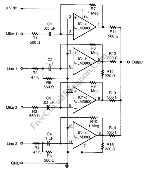
This audio mixer circuit does not utilize a low impedance input to mix non-ideal sources; instead, it employs multiple amplifiers to provide ideal sources prior to mixing through simple resistors. An ideal source is characterized by low impedances, which...
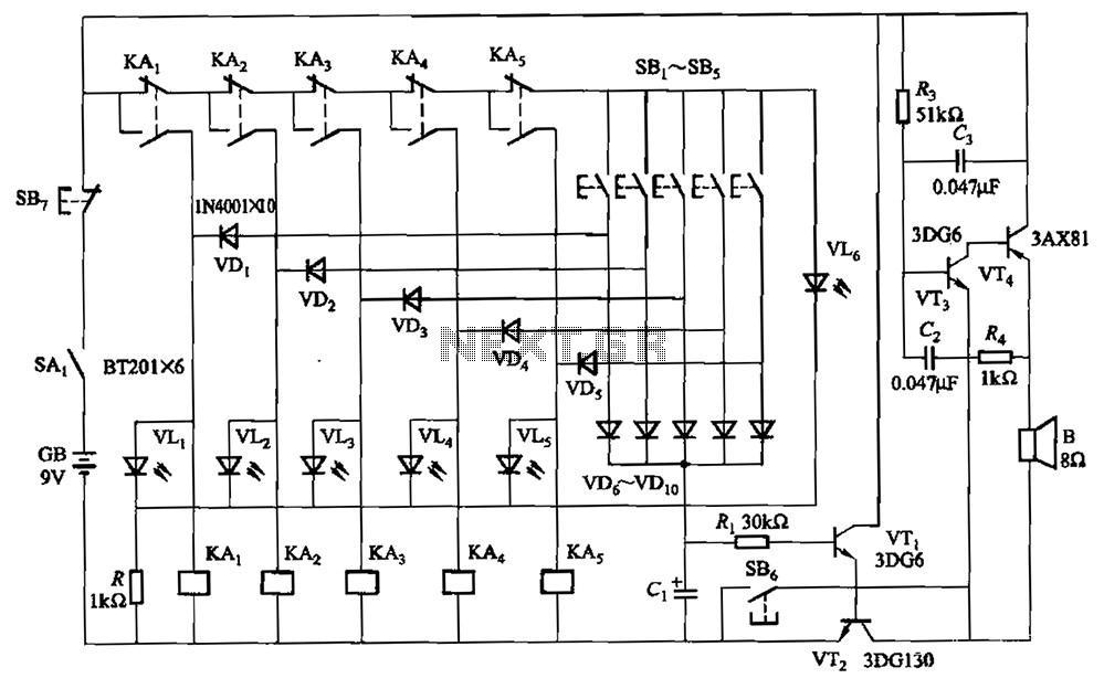
A relay-style circuit designed for a five electronic responder group. This circuit features self-locking capabilities, sound and light displays, time monitoring, and additional functions. The circuit includes a monitoring time button operated by the moderator. When this button is...
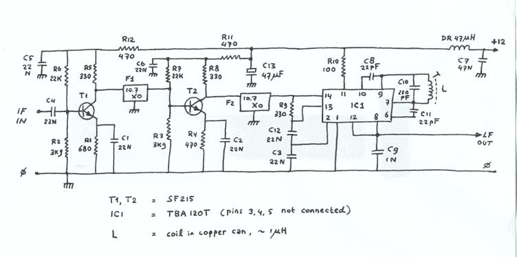
Two conventional amplifier stages built with SF215 transistors are linked by ceramic 10.7MHz IF filters, and followed by an FM demodulator built with a TBA120T i.c. Straight from the databook. Output goes via a 100k log potmeter (not shown)...
More: A comprehensive electronic schematic description is required to provide an overview of the circuit's functionality, components, and operation. The schematic should include a clear representation of the electronic components involved, such as resistors, capacitors, diodes, transistors, integrated circuits,...
This circuit is designed to detect incoming calls on a cellular phone, even when the phone's ringer is turned off, by utilizing a flashing LED. The device should be positioned a few centimeters away from the cellular phone, allowing...
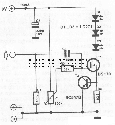
The transmitter provides an optical link (infrared) for headphones. Three infrared LEDs (IR) are powered by T1, with P1 used to adjust the current level. The current consumption of this headphones infrared transmitter is approximately 60mA at 9V. The infrared...