
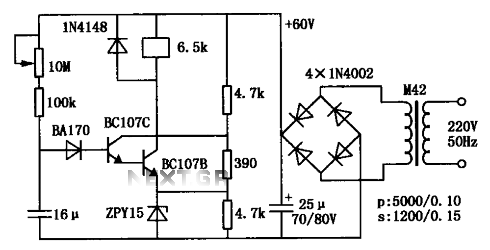
An attenuated tone control circuit diagram
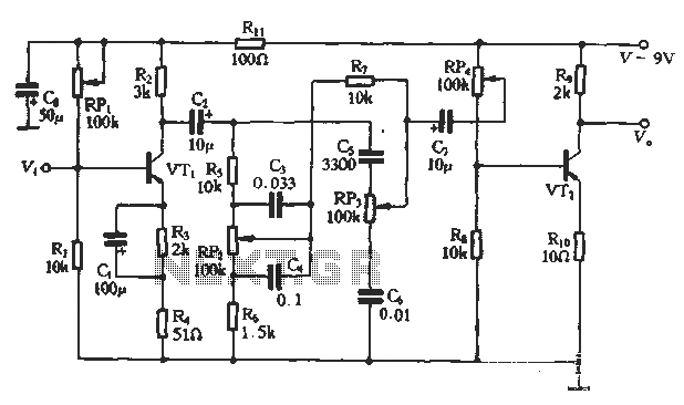
The attenuated tone control circuit is designed to provide adjustable bass and treble control for audio applications. The circuit employs two potentiometers: one for bass adjustment (RP2) and another for treble adjustment (RP3). The use of transistors Q and VT2 allows for amplification and control of the audio signal, while the RC networks formed by the capacitors and resistors are critical for shaping the frequency response.
In the bass control section, the interaction between capacitor C3 and resistor R5 plays a pivotal role. When the bass potentiometer is adjusted, the impedance changes, affecting how much of the bass signal is allowed to pass through. The design ensures that at lower settings, the bass is attenuated, providing a more balanced audio output.
For the treble control, the circuit utilizes capacitor C5 and resistor RP3 to manage high-frequency signals. The smaller capacitance of C5 allows for the passage of treble frequencies while effectively blocking bass frequencies. The additional filtering introduced by capacitor C6 and resistor RP3 further enhances the treble output, providing a clear and crisp sound.
Overall, this attenuated tone control circuit is an effective solution for adjusting audio frequencies, allowing users to tailor their listening experience by managing the balance between bass and treble. The careful selection of component values and the arrangement of the circuit elements ensure that the desired audio characteristics are achieved, making it suitable for various audio applications.This article is an attenuated tone control circuit diagram. This circuit is mainly composed of transistors and RC networks are network components. As shown below, since the C4, R shunt effect, the high-frequency component is very attenuated relative to enhance the bass. When the sliding contact potentiometer located at the lower end, C is short-circuited, the audio signal Q, R5, C3, VTz horses to the base, and C since the Q series, due to the smaller capacity of C3, the larger of the bass signal exhibits capacitance, bass difficult to pass, so the bass is attenuated, so RP2 bass played a role in the control.
Foundation designed treble control potentiometer, when the foundation designed sliding contact potentiometer located at the upper end, the audio signal is sent to Pakistan and c5 series VT2 base. Since / C5 capacity is small, the capacitance of the great bass, bass is not passed, while the treble can be passed.
But also because after RP3 and C6 series impedance is large, bypassing much of the treble, so relatively enhance the treble. When the puzzle, sliding potentiometer point located at the lower end, treble attenuation due by RP3 and C6 bypass weakened, so that the treble was attenuated.
Related Circuits
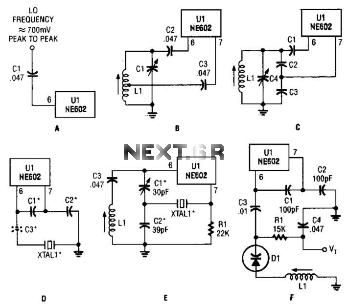
Any standard oscillator, such as a Colpitts or Hartley configuration, can be utilized to generate the local oscillator (LO) frequency required by the NE602. The NE602 is a versatile integrated circuit commonly used in radio frequency applications, particularly in mixer...
For a robot to perform its assigned tasks, a controller is necessary. This controller may be mechanical, electrical, electronic, or a combination of these. It acts as the brain of the entire system, providing the robot with its intelligence....
This 555 timer circuit temperature monitoring system project can monitor temperature at up to four points. The system allows for the selection of whether the alarm should be triggered when the temperature increases or decreases, depending on the resistance...
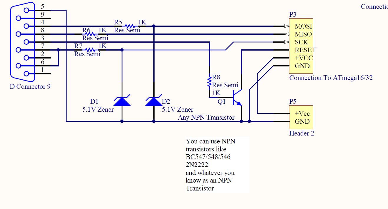
ISP programmer with circuit diagram for AVR Atmega32 microcontroller. This ISP burner circuit is an adaptation of the Pony programmer and uses PonyProg software. The ISP (In-System Programming) programmer designed for the AVR Atmega32 microcontroller facilitates the programming of the...
The circuit is straightforward yet capable of outstanding performance. It has been specifically designed as an amplifier for the digital sound card in a computer. Audio input can be sourced from any two-channel line-level device such as a television,...
The circuit is a relay delay pull transistor configuration. Initially, when powered, the 16 µF capacitor has a voltage of zero, resulting in both transistors being off, and the relay remains inactive. As the 16 µF capacitor charges over...