
Analogue Tachometer and Dwellmeter
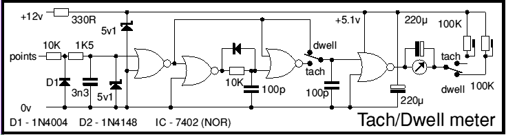
The circuit in question utilizes a TTL (Transistor-Transistor Logic) quad NOR gate, which consists of four independent NOR gates integrated into a single package. The NOR gate is a fundamental building block in digital electronics, known for its versatility in constructing various logical functions. The use of a quad configuration allows for multiple logical operations to be performed within a compact design, enhancing circuit efficiency and reducing component count.
In this specific design, the input signals are fed into the NOR gates, which produce an output that is the logical negation of the OR operation. This means that the output will be high (logic level '1') only when all inputs are low (logic level '0'). This characteristic is particularly useful in applications requiring signal inversion or in creating complex logic circuits through cascading multiple NOR gates.
While the original design utilizes TTL technology, it is noted that CMOS (Complementary Metal-Oxide-Semiconductor) technology could also be employed. CMOS offers advantages such as lower power consumption and higher noise immunity, making it suitable for battery-operated devices and applications where energy efficiency is paramount. When designing with CMOS, care must be taken to ensure that the input voltage levels are compatible with the logic family being used, as TTL and CMOS have different voltage thresholds.
The circuit can serve in various applications, including oscillators, pulse generators, and as part of larger digital systems. Its straightforward implementation allows for easy integration into existing designs, making it a valuable addition to any electronics engineer's toolkit.This circuit as first published in Wireless World September 1975 and subsequently in MECRM. It's built around a TTL quad NOR gate, though CMOS could be used. 🔗 External reference
Related Circuits
This design circuit is a tachometer circuit based on the LM2907 integrated circuit, which can provide zero-crossing data to a digital system. At each zero crossing of the input signal, the charge pump alters the state of capacitor C1...
The operation of the converter relies on the weighted addition and transfer of the analog input levels to the digital output levels. It comprises comparators and resistors. Although, theoretically, the number of bits is unlimited, each bit requires a...
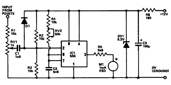
The following circuit illustrates a Tachometer Circuit Project. This circuit is constructed using the 555 Timer IC. Features include a monostable IC and voltage capabilities. The Tachometer Circuit utilizes a 555 Timer configured in monostable mode to measure the rotational...
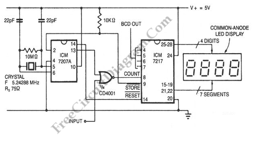
For convenient reading, the display of this tachometer circuit shows the reading in hertz directly. The conversion time will be equal to the gating time. The tachometer circuit is designed to provide a direct digital readout of rotational speed in...
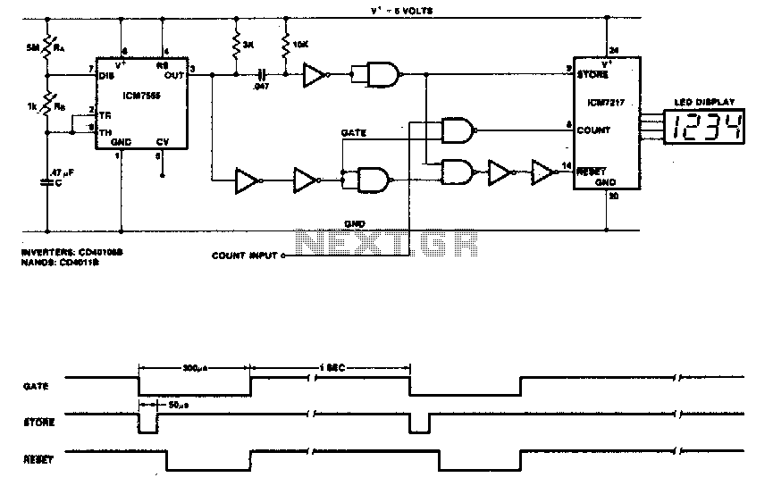
This circuit utilizes the low-power ICM7555 (CMOS 555) to generate the gating, STORE, and RESET signals. The timer is configured as an astable multivibrator to provide the gating signal. Calibration of the system is achieved using a 5 MΩ...
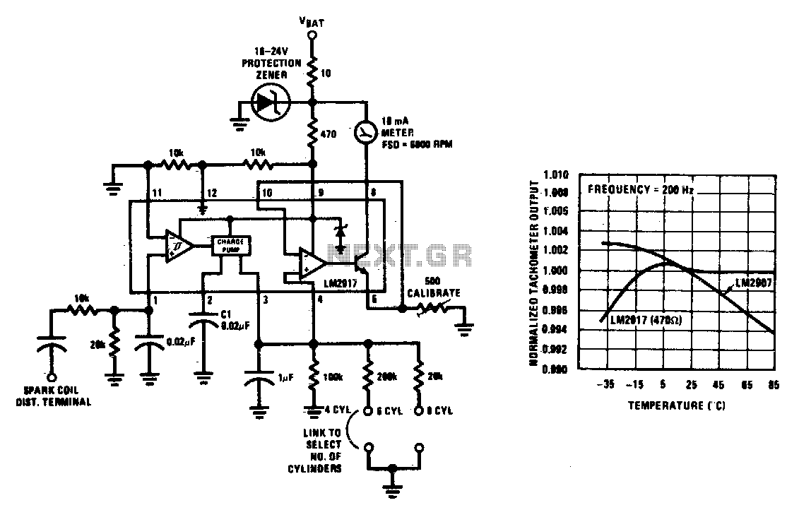
This tachometer can be configured for any number of cylinders by connecting the appropriate timing resistor as illustrated. A 500-ohm trim resistor can be utilized for final calibration. Additionally, a protection circuit consisting of a 10-ohm resistor and a...