
Astable flip-flop multivibrator circuit
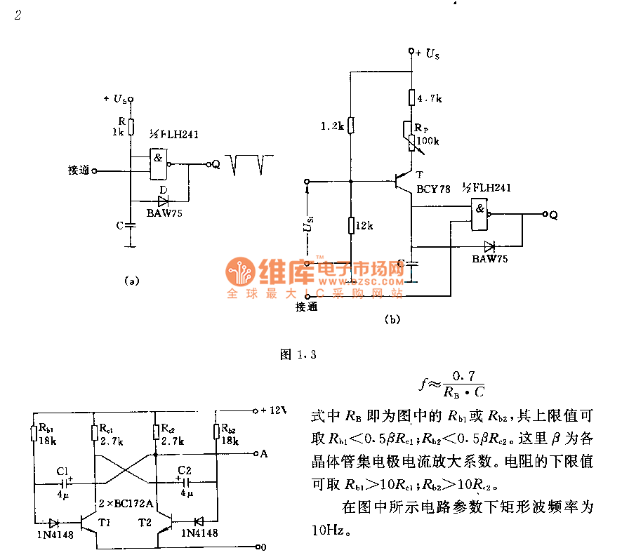
The circuit is designed to produce a square wave output, which can be utilized in various applications such as clock signals for digital circuits or timing applications. The frequency of the output waveform is inversely proportional to the product of the resistance value (RB) and the capacitance (C). This relationship indicates that by adjusting either the resistance or capacitance, the frequency of the output can be modified, allowing for flexibility in circuit design.
The parameters Rb1 and Rb2 are critical in ensuring that the output maintains the desired characteristics. The condition that Rb1 must be less than 0.5 times RC1 and Rb2 must be less than 0.5 times RC2 ensures that the circuit operates within safe limits to prevent distortion of the waveform and to maintain the integrity of the signal. The transistor's current amplification factor, ?, also plays a vital role in defining the gain of the circuit, influencing how effectively the circuit can drive loads connected to the output.
In practical applications, careful selection of the values for RB and C is necessary to achieve the desired frequency and ensure the circuit's reliability. The design should also consider the power ratings of the components to prevent overheating and failure during operation. Proper decoupling and filtering techniques may also be implemented to minimize noise in the output signal, enhancing the performance of the circuit in sensitive applications.The two parts` component parameters and models of the circuit are corresponding to simultaneously obtain a rectangular wave with duty ratio of 1:1, its frequency f = 0.7/RB ¢ C. RB is Rb1 or Rb2 in the figure, and its upper limit value Rb1 < 0.5?RC1 ; Rb2 < 0.5?RC2, here ? is the transistor collector current amplification factor. The lower lim.. 🔗 External reference
Related Circuits
This schematic requires clarification. It is assumed that pin 2 is connected by a wire to pin 6, although this connection appears to be unclear. The circuit in question involves a schematic where pin 2 and pin 6 are interconnected....
The circuit for the photoelectric switch S1 functions as a control switch for the luggage room light. In its closed operating state, the voltage is positive. If S2 is closed, irrespective of the state of S1, the output terminal...
This power supply utilizes a single 7812 IC voltage regulator along with multiple external pass transistors, enabling it to deliver output load currents of up to 30 amps. The circuit design incorporates a 7812 linear voltage regulator, which is...
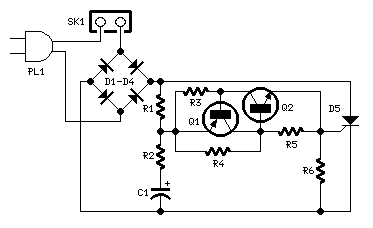
This is a 220V LED flasher circuit designed as a reliable alternative to thermally activated switches used for flashing Christmas tree lamps. It is a cost-effective and easy-to-assemble circuit. The components include R1 (100K), R2 (1K), R5 (1K), R3...

The circuit indicates two different water temperature trip points by activating LEDs when the specified temperatures are reached. It is built around the LM2904 dual operational amplifier, which is powered by a 12 V automotive system. A thermistor is...

This is an economical 150 Watt amplifier circuit featuring two Darlington power transistors, TIP 142 and TIP 147. The circuit is capable of delivering up to 150 W RMS to a 4 Ohm speaker, providing substantial audio output. The...
Warning: include(partials/cookie-banner.php): Failed to open stream: Permission denied in /var/www/html/nextgr/view-circuit.php on line 713
Warning: include(): Failed opening 'partials/cookie-banner.php' for inclusion (include_path='.:/usr/share/php') in /var/www/html/nextgr/view-circuit.php on line 713